EVAL-AD5443-DBRDZ Analog Devices Inc, EVAL-AD5443-DBRDZ Datasheet - Page 6
EVAL-AD5443-DBRDZ
Manufacturer Part Number
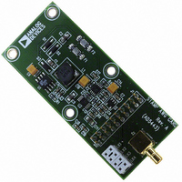
EVAL-AD5443-DBRDZ
Description
BOARD EVAL CARD CLINUX/STAMP
Manufacturer
Analog Devices Inc
Datasheet
1.AD5443YRMZ.pdf
(28 pages)
Specifications of EVAL-AD5443-DBRDZ
Number Of Dac's
1
Number Of Bits
12
Outputs And Type
1, Differential
Sampling Rate (per Second)
2.5M
Data Interface
Serial
Settling Time
50ns
Dac Type
Current
Voltage Supply Source
Single
Operating Temperature
-40°C ~ 125°C
Utilized Ic / Part
AD5443
Silicon Manufacturer
Analog Devices
Application Sub Type
DAC
Kit Application Type
Data Converter
Silicon Core Number
AD5443
Kit Contents
Board
Development Tool Type
Hardware - Eval/Demo Board
Rohs Compliant
Yes
Lead Free Status / RoHS Status
Lead free / RoHS Compliant


AD5426/AD5432/AD5443
ABSOLUTE MAXIMUM RATINGS
Transient currents of up to 100 mA do not cause SCR latch-up.
T
Table 3.
Parameter
V
V
I
Logic Inputs and Output
Operating Temperature Range
Storage Temperature Range
Junction Temperature
10-lead MSOP θ
Lead Temperature, Soldering (10 sec)
IR Reflow, Peak Temperature (<20 sec)
1
ESD CAUTION
ESD (electrostatic discharge) sensitive device. Electrostatic charges as high as 4000 V readily accumulate on the
human body and test equipment and can discharge without detection. Although this product features
proprietary ESD protection circuitry, permanent damage may occur on devices subjected to high energy
electrostatic discharges. Therefore, proper ESD precautions are recommended to avoid performance
degradation or loss of functionality.
OUT
Overvoltages at SCLK, SYNC , and DIN are clamped by internal diodes.
DD
REF
A
Extended Industrial (Y Version)
= 25°C, unless otherwise noted.
1, I
, R
to GND
FB
OUT
to GND
2 to GND
JA
Thermal Impedance
1
Rating
−0.3 V to +7 V
−12 V to +12 V
−0.3 V to V
−0.3 V to V
−40°C to +125°C
−65°C to +150°C
150°C
206°C/W
300°C
235°C
DD
DD
+ 0.3 V
+ 0.3 V
Rev. C | Page 6 of 28
Stresses above those listed under Absolute Maximum Ratings
may cause permanent damage to the device. This is a stress
rating only and functional operation of the device at these or
any other conditions above those indicated in the operational
section of this specification is not implied. Exposure to absolute
maximum rating conditions for extended periods may affect
device reliability.
TO OUTPUT PIN
Figure 4. Load Circuit for SDO Timing Specifications
20pF
C
L
200μA
200μA
I
I
OL
OH
V
OH (MIN)
+ V
2
OL (MAX)
Related parts for EVAL-AD5443-DBRDZ
Image
Part Number
Description
Manufacturer
Datasheet
Request
R

Part Number:
Description:
IC, ADJ LDO REG, 1.5V TO 5V 250mA MSOP-8
Manufacturer:
Vishay
Datasheet:

Part Number:
Description:
IC, ADJ LDO REG, 1.5V TO 5V 0.6A 8-TSSOP
Manufacturer:
Vishay
Datasheet:
Part Number:
Description:
IC, ADJ LDO REG, 1.5V TO 5V 250mA MSOP-8
Manufacturer:
Vishay
Datasheet:

Part Number:
Description:
IC ADJ LDO REG 1.5V TO 5V 150mA 5-SOT-23
Manufacturer:
Vishay
Datasheet:

Part Number:
Description:
BOARD EVAL AS1324-AD
Manufacturer:
austriamicrosystems
Datasheet:
Part Number:
Description:
IC, ADJ LDO REG, 1.5V TO 5V 0.6A 8-TSSOP
Manufacturer:
Vishay
Datasheet:

Part Number:
Description:
IC, ADJ LDO REG, 1.5V TO 5V, 0.3A, MSOP8
Manufacturer:
Vishay
Datasheet:
Part Number:
Description:
IC, ADJ LDO REG, 1.5V TO 5V, 0.3A, MSOP8
Manufacturer:
Vishay
Datasheet:
Part Number:
Description:
IC, ADJ LDO REG 1.215V TO 5V 0.3A MSOP-8
Manufacturer:
Vishay
Datasheet:
Part Number:
Description:
IC, ADJ LDO REG 1.215V TO 5V 0.3A MSOP-8
Manufacturer:
Vishay
Datasheet:

Part Number:
Description:
±1.7g Dual-Axis IMEMS Accelerometer Evaluation Board
Manufacturer:
Analog Devices Inc
Datasheet:

Part Number:
Description:
IC MULTIPLIER ANALOG 8-SOIC T/R
Manufacturer:
Analog Devices Inc
Datasheet:

Part Number:
Description:
IC ANALOG MULTIPLIER 8-DIP
Manufacturer:
Analog Devices Inc
Datasheet:
Part Number:
Description:
IC ANALOG MULTIPLIER 8-SOIC
Manufacturer:
Analog Devices Inc
Datasheet:
Part Number:
Description:
IC ANALOG MULTIPLIER 8-DIP
Manufacturer:
Analog Devices Inc
Datasheet: