EVAL-AD5429EBZ Analog Devices Inc, EVAL-AD5429EBZ Datasheet - Page 8
EVAL-AD5429EBZ
Manufacturer Part Number
EVAL-AD5429EBZ
Description
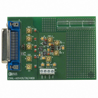
BOARD EVALUATION FOR AD5429
Manufacturer
Analog Devices Inc
Specifications of EVAL-AD5429EBZ
Number Of Dac's
2
Number Of Bits
8
Outputs And Type
2, Single Ended
Sampling Rate (per Second)
2.47M
Data Interface
Serial
Settling Time
30ns
Dac Type
Current
Voltage Supply Source
Single
Operating Temperature
-40°C ~ 125°C
Utilized Ic / Part
AD5429
Lead Free Status / RoHS Status
Lead free / RoHS Compliant


AD5429/AD5439/AD5449
PIN CONFIGURATION AND FUNCTION DESCRIPTIONS
Table 4. Pin Function Descriptions
Pin No.
1
2
3
4
5
6
7
8
9
10
11
12
13
14
15
16
Mnemonic
I
I
R
V
GND
LDAC
SCLK
SDIN
SDO
SYNC
CLR
V
V
R
I
I
OUT
OUT
OUT
OUT
FB
FB
REF
DD
REF
A
B
1A
2A
2B
1B
A
B
Description
Ground Pin.
input. Alternatively, by means of the serial control bits, the device can be configured such that data is clocked
into the shift register on the rising edge of SCLK.
DAC A Current Output.
DAC A Analog Ground. This pin should typically be tied to the analog ground of the system, but it can be
biased to achieve single-supply operation.
DAC Feedback Resistor Pin. This pin establishes voltage output for the DAC by connecting to an external
amplifier output.
DAC A Reference Voltage Input Pin.
Load DAC Input. This pin allows asynchronous or synchronous updates to the DAC output. The DAC is
asynchronously updated when this signal goes low. Alternatively, if this line is held permanently low, an
automatic or synchronous update mode is selected, whereby the DAC is updated on the 16th clock falling
edge when the device is in standalone mode, or on the rising edge of SYNC when in daisy-chain mode.
Serial Clock Input. By default, data is clocked into the input shift register on the falling edge of the serial clock
Serial Data Input. Data is clocked into the 16-bit input register on the active edge of the serial clock input. By
default, data is clocked at power-on into the shift register on the falling edge of SCLK. The control bits allow
the user to change the active edge to a rising edge.
Serial Data Output. This pin allows a number of parts to be daisy-chained. By default, data is clocked into the
shift register on the falling edge and clocked out via SDO on the rising edge of SCLK. Data is always clocked
out on the alternate edge to loading data to the shift register. Writing the readback control word to the shift
register makes the DAC register contents available for readback on the SDO pin, and they are clocked out on the
next 16 opposite clock edges to the active clock edge.
Active Low Control Input. This pin provides the frame synchronization signal for the input data. When SYNC
goes low, it powers on the SCLK and DIN buffers, and the input shift register is enabled. Data is loaded into the
shift register on the active edge of the subsequent clocks. In standalone mode, the serial interface counts the
clocks, and data is latched into the shift register on the 16th active clock edge.
Active Low Control Input. This pin clears the DAC output, input, and DAC registers. Configuration mode allows the
user to enable the hardware CLR pin as a clear-to-zero scale or midscale, as required.
Positive Power Supply Input. These parts can be operated from a supply of 2.5 V to 5.5 V.
DAC B Reference Voltage Input Pin.
DAC B Feedback Resistor Pin. This pin establishes voltage output for the DAC by connecting to an external
amplifier output.
DAC B Analog Ground. This pin typically should be tied to the analog ground of the system, but it can be
biased to achieve single-supply operation.
DAC B Current Output.
I
I
OUT
OUT
V
LDAC
SCLK
R
REF
SDIN
GND
FB
1A
2A
A
A
Figure 6. Pin Configuration
1
2
3
4
5
6
7
8
NC = NO CONNECT
Rev. C | Page 8 of 32
(Not to Scale)
AD5429/
AD5439/
AD5449
TOP VIEW
16
15
14
13
12
11
10
9
I
I
R
V
V
CLR
SYNC
SDO
OUT
OUT
REF
DD
FB
B
1B
2B
B
Related parts for EVAL-AD5429EBZ
Image
Part Number
Description
Manufacturer
Datasheet
Request
R


Part Number:
Description:
BOARD EVAL FOR SI270X-A
Manufacturer:
Silicon Laboratories Inc
Datasheet:

Part Number:
Description:
BUCK CONV REF DESIGN KIT IP1201
Manufacturer:
International Rectifier
Datasheet:
Part Number:
Description:
BOARD DEMO SYNC DUAL BUCK CNVTER
Manufacturer:
International Rectifier
Datasheet:
Part Number:
Description:
BOARD DEMO SYNC BUCK CONVETER
Manufacturer:
International Rectifier
Datasheet:

Part Number:
Description:
EVALBOARD/EB Omnidirectional microphone - Analog
Manufacturer:
Analog Devices
Datasheet:
Part Number:
Description:
EVALBOARD/EB Omnidirectional microphone - Analog
Manufacturer:
Analog Devices
Datasheet:


Part Number:
Description:
BOARD EVAL LED DRIVER LT3756
Manufacturer:
Linear Technology
Datasheet:

Part Number:
Description:
BOARD EVAL FOR AD7741/7742
Manufacturer:
Analog Devices Inc
Datasheet:

Part Number:
Description:
±1.7g Dual-Axis IMEMS Accelerometer Evaluation Board
Manufacturer:
Analog Devices Inc
Datasheet:

Part Number:
Description:
IC MULTIPLIER ANALOG 8-SOIC T/R
Manufacturer:
Analog Devices Inc
Datasheet:

Part Number:
Description:
IC ANALOG MULTIPLIER 8-DIP
Manufacturer:
Analog Devices Inc
Datasheet:
Part Number:
Description:
IC ANALOG MULTIPLIER 8-SOIC
Manufacturer:
Analog Devices Inc
Datasheet:
Part Number:
Description:
IC ANALOG MULTIPLIER 8-DIP
Manufacturer:
Analog Devices Inc
Datasheet: