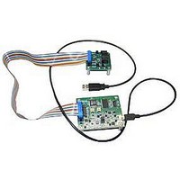
EVAL-AD5422EBZ Analog Devices Inc, EVAL-AD5422EBZ Datasheet - Page 33
EVAL-AD5422EBZ
Manufacturer Part Number
EVAL-AD5422EBZ
Description
BOARD EVAL FOR AD5422
Manufacturer
Analog Devices Inc
Specifications of EVAL-AD5422EBZ
Number Of Dac's
1
Number Of Bits
16
Outputs And Type
1, Single Ended
Sampling Rate (per Second)
1M
Data Interface
Serial
Settling Time
32µs
Dac Type
Current/Voltage
Voltage Supply Source
Analog and Digital, Dual ±
Operating Temperature
-40°C ~ 85°C
Utilized Ic / Part
AD5422
Silicon Manufacturer
Analog Devices
Application Sub Type
DAC
Kit Application Type
Data Converter
Silicon Core Number
AD5422
Kit Contents
Board And Literature
Lead Free Status / RoHS Status
Lead free / RoHS Compliant


AD5410/AD5420 registers. The update clock frequency for any
given value is the same for all output ranges. The step size,
however, varies across output ranges for a given value of step
size because the LSB size is different for each output range.
Table 24 shows the range of programmable slew times for a full-
scale change on any of the output ranges. The values in Table 24
were obtained using Equation 1.
The digital slew rate control feature results in a staircase
formation on the current output, as shown in Figure 72. This
figure also shows how the staircase can be removed by
connecting capacitors to the CAP1 and CAP2 pins, as described
in the I
I
Capacitors can be placed between CAP1 and AV
and AV
The CAP1 and CAP2 pins are available only on the LFCSP
package. The capacitors form a filter on the current output
circuitry, as shown in Figure 70, reducing the bandwidth and
the slew rate of the output current. Figure 71 shows the effect
the capacitors have on the slew rate of the output current. To
achieve significant reductions in the rate of change, very large
capacitor values are required, which may not be suitable in
some applications. In this case, the digital slew rate control
OUT
Figure 68. Output Current Slewing Under Control of the Digital Slew Rate
FILTERING CAPACITORS (LFCSP PACKAGE)
OUT
25
20
15
10
DD
5
0
–10
, as shown in Figure 69.
Filtering Capacitors (LFCSP Package) section.
T
AV
R
A
LOAD
0
DD
= 25°C
= 24V
10
= 300Ω
Figure 69. I
AD5412/
AD5422
10ms RAMP, SR CLOCK = 0x1, SR STEP = 0x5
50ms RAMP, SR CLOCK = 0xA, SR STEP = 0x7
100ms RAMP, SR CLOCK = 0x8, SR STEP = 0x5
20
AV
GND
30
Control Feature
DD
OUT
40
CAP1
CAP2
Filtering Capacitors
TIME (ms)
I
AV
OUT
DD
50
60
C1
70
C2
80
DD
90
, and CAP2
100 110
Rev. C | Page 33 of 40
feature can be used. The capacitors can be used in conjunction
with the digital slew rate control feature as a means of
smoothing out the steps caused by the digital code increments,
as shown in Figure 72.
Figure 71. Slew Controlled 4 mA to 20 mA Output Current Step Using
Figure 72. Smoothing Out the Steps Caused by the Digital Slew
DAC
25
20
15
10
6.8
6.7
6.6
6.5
6.4
6.3
6.2
6.1
5
0
–0.5
–1
External Capacitors on the CAP1 and CAP2 Pins
0
0
T
AV
R
0.5
A
LOAD
Figure 70. I
1
DD
= 25°C
= 24V
4kΩ
Rate Control Feature
= 300Ω
CAP1
1.0
2
NO CAPACITOR
10nF ON CAP1
10nF ON CAP2
47nF ON CAP1
47nF ON CAP2
R1
OUT
TIME (ms)
12.5kΩ
1.5
TIME (ms)
3
Filter Circuitry
2.0
CAP2
4
NO EXTERNAL CAPS
10nF ON CAP1
10nF ON CAP2
AD5412/AD5422
2.5
C1
C2
5
T
AV
R
A
LOAD
40Ω
3.0
DD
= 25°C
6
= 24V
= 300Ω
AV
3.5
DD
7
BOOST
I
4.0
OUT
8
Related parts for EVAL-AD5422EBZ
Image
Part Number
Description
Manufacturer
Datasheet
Request
R


Part Number:
Description:
BOARD EVAL FOR SI270X-A
Manufacturer:
Silicon Laboratories Inc
Datasheet:

Part Number:
Description:
BUCK CONV REF DESIGN KIT IP1201
Manufacturer:
International Rectifier
Datasheet:
Part Number:
Description:
BOARD DEMO SYNC DUAL BUCK CNVTER
Manufacturer:
International Rectifier
Datasheet:
Part Number:
Description:
BOARD DEMO SYNC BUCK CONVETER
Manufacturer:
International Rectifier
Datasheet:

Part Number:
Description:
EVALBOARD/EB Omnidirectional microphone - Analog
Manufacturer:
Analog Devices
Datasheet:
Part Number:
Description:
EVALBOARD/EB Omnidirectional microphone - Analog
Manufacturer:
Analog Devices
Datasheet:


Part Number:
Description:
BOARD EVAL LED DRIVER LT3756
Manufacturer:
Linear Technology
Datasheet:

Part Number:
Description:
BOARD EVAL FOR AD7741/7742
Manufacturer:
Analog Devices Inc
Datasheet:

Part Number:
Description:
±1.7g Dual-Axis IMEMS Accelerometer Evaluation Board
Manufacturer:
Analog Devices Inc
Datasheet:

Part Number:
Description:
IC MULTIPLIER ANALOG 8-SOIC T/R
Manufacturer:
Analog Devices Inc
Datasheet:

Part Number:
Description:
IC ANALOG MULTIPLIER 8-DIP
Manufacturer:
Analog Devices Inc
Datasheet:
Part Number:
Description:
IC ANALOG MULTIPLIER 8-SOIC
Manufacturer:
Analog Devices Inc
Datasheet:
Part Number:
Description:
IC ANALOG MULTIPLIER 8-DIP
Manufacturer:
Analog Devices Inc
Datasheet: