EVAL-AD5422EBZ Analog Devices Inc, EVAL-AD5422EBZ Datasheet - Page 8
EVAL-AD5422EBZ
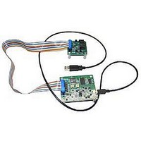
Manufacturer Part Number
EVAL-AD5422EBZ
Description
BOARD EVAL FOR AD5422
Manufacturer
Analog Devices Inc
Specifications of EVAL-AD5422EBZ
Number Of Dac's
1
Number Of Bits
16
Outputs And Type
1, Single Ended
Sampling Rate (per Second)
1M
Data Interface
Serial
Settling Time
32µs
Dac Type
Current/Voltage
Voltage Supply Source
Analog and Digital, Dual ±
Operating Temperature
-40°C ~ 85°C
Utilized Ic / Part
AD5422
Silicon Manufacturer
Analog Devices
Application Sub Type
DAC
Kit Application Type
Data Converter
Silicon Core Number
AD5422
Kit Contents
Board And Literature
Lead Free Status / RoHS Status
Lead free / RoHS Compliant


AD5412/AD5422
TIMING CHARACTERISTICS
AV
V
Table 4.
Parameter
WRITE MODE
READBACK MODE
DAISY-CHAIN MODE
1
2
3
4
Guaranteed by characterization; not production tested.
All input signals are specified with t
See Figure 2, Figure 3, and Figure 4.
C
t
t
t
t
t
t
t
t
t
t
t
t
t
t
t
t
t
t
t
t
t
t
t
t
t
t
t
t
t
t
OUT
1
2
3
4
5
5
6
7
8
9
10
11
12
13
14
15
16
17
18
19
20
21
22
23
24
25
26
27
28
29
L SDO
DD
: R
= capacitive load on SDO output.
= 10.8 V to 26.4 V, AV
LOAD
1, 2, 3
= 1 kΩ, C
L
= 200 pF, I
Limit at T
33
13
13
13
40
5
5
5
40
20
5
90
40
40
13
40
5
5
40
35
35
90
40
40
13
40
5
5
40
35
SS
= −26.4 V to −3 V/0 V, AV
R
= t
MIN
F
OUT
= 5 ns (10% to 90% of DV
, T
: R
MAX
LOAD
= 300 Ω; all specifications T
Unit
ns min
ns min
ns min
ns min
ns min
μs min
ns min
ns min
ns min
ns min
μs max
ns min
ns min
ns min
ns min
ns min
ns min
ns min
ns min
ns max
ns max
ns min
ns min
ns min
ns min
ns min
ns min
ns min
ns min
ns max
CC
) and timed from a voltage level of 1.2 V.
DD
+ |AV
Rev. C | Page 8 of 40
Description
SCLK cycle time
SCLK low time
SCLK high time
LATCH delay time
LATCH high time
LATCH high time (after a write to the control register)
Data setup time
Data hold time
LATCH low time
CLEAR pulse width
CLEAR activation time
SCLK cycle time
SCLK low time
SCLK high time
LATCH delay time
LATCH high time
Data setup time
Data hold time
LATCH low time
Serial output delay time (C
LATCH rising edge to SDO tristate (C
SCLK cycle time
SCLK low time
SCLK high time
LATCH delay time
LATCH high time
Data setup time
Data hold time
LATCH low time
Serial output delay time (C
SS
| < 52.8V, GND = 0 V, REFIN = +5 V external; DV
MIN
to T
MAX
, unless otherwise noted.
L SDO
L SDO
4
4
= 15 pF)
= 15 pF)
L SDO
4
= 15 pF)
CC
= 2.7 V to 5.5 V.
Related parts for EVAL-AD5422EBZ
Image
Part Number
Description
Manufacturer
Datasheet
Request
R


Part Number:
Description:
BOARD EVAL FOR SI270X-A
Manufacturer:
Silicon Laboratories Inc
Datasheet:

Part Number:
Description:
BUCK CONV REF DESIGN KIT IP1201
Manufacturer:
International Rectifier
Datasheet:
Part Number:
Description:
BOARD DEMO SYNC DUAL BUCK CNVTER
Manufacturer:
International Rectifier
Datasheet:
Part Number:
Description:
BOARD DEMO SYNC BUCK CONVETER
Manufacturer:
International Rectifier
Datasheet:

Part Number:
Description:
EVALBOARD/EB Omnidirectional microphone - Analog
Manufacturer:
Analog Devices
Datasheet:
Part Number:
Description:
EVALBOARD/EB Omnidirectional microphone - Analog
Manufacturer:
Analog Devices
Datasheet:


Part Number:
Description:
BOARD EVAL LED DRIVER LT3756
Manufacturer:
Linear Technology
Datasheet:

Part Number:
Description:
BOARD EVAL FOR AD7741/7742
Manufacturer:
Analog Devices Inc
Datasheet:

Part Number:
Description:
±1.7g Dual-Axis IMEMS Accelerometer Evaluation Board
Manufacturer:
Analog Devices Inc
Datasheet:

Part Number:
Description:
IC MULTIPLIER ANALOG 8-SOIC T/R
Manufacturer:
Analog Devices Inc
Datasheet:

Part Number:
Description:
IC ANALOG MULTIPLIER 8-DIP
Manufacturer:
Analog Devices Inc
Datasheet:
Part Number:
Description:
IC ANALOG MULTIPLIER 8-SOIC
Manufacturer:
Analog Devices Inc
Datasheet:
Part Number:
Description:
IC ANALOG MULTIPLIER 8-DIP
Manufacturer:
Analog Devices Inc
Datasheet: