NCP5602EVB ON Semiconductor, NCP5602EVB Datasheet
NCP5602EVB
Specifications of NCP5602EVB


Related parts for NCP5602EVB

NCP5602EVB Summary of contents
Page 1
NCP5602 High Efficiency Ultra Small Thinnest White LED Driver The NCP5602 product is a dual output LED driver dedicated to the LCD display backlighting. The built−in DC−DC converter is based on a high efficient charge pump structure with operating mode ...
Page 2
Vbat C3 11 GND 1 mF/6.3 V SCL 6 DIGITAL CONTROL SDA 5 Vbat R1 GND 4 100 k ANALOG CONTROL 1 GND OVERTEMPERATURE C2 C1 220 nF 220 CHARGE PUMP DC−DC CONVERTER OVERVOLTAGE Vbat Q1 ...
Page 3
PIN FUNCTION DESCRIPTION Pin No. Symbol Function 1 GND POWER 2 LED1 INPUT, POWER 3 LED2 INPUT, POWER 4 I INPUT, ANALOG REF 5 SDA INPUT, DIGITAL 6 SCL INPUT, DIGITAL 7 VOUT OUTPUT, POWER 8 C2P POWER 9 C2N ...
Page 4
MAXIMUM RATINGS Rating Power Supply Output Power Supply Digital Input Voltage Digital Input Current Human Body Model 1500 100 pF (Note 3) Machine Model LLGA12 Package Power Dissipation @ T = +85°C (Note 4) A ...
Page 5
POWER SUPPLY SECTION (Typical values are referenced to T temperature, operating conditions 2.85 V < Vbat < 5.5 V, unless otherwise noted.) Rating Power Supply Continuous DC Current in the Load @ Vf = 3.0 V, ICON = L @ ...
Page 6
DC−DC Operation The converter is based on a charge pump technique to generate a DC voltage capable to supply the White LED load. The system regulates the current flowing into each LED by means of internal current mirrors associated with ...
Page 7
Finally, an external network can be connected across Vout and ground , but the current through such network will not be regulated by the NCP5602 chip (see Figure 5). On I2C Protocol The standard I2C protocol is used to transfer ...
Page 8
The physical address of the NCP5602 is 1001 111X, the X being the Read/Write identifier as defined by the I2C specification. Since the NCP5602 does not return data, the first byte of the I2C frame shall be 1001 1110 ($9E) ...
Page 9
When the ICON mode is activated, the DC−DC converter is switched OFF, LED#1 is deactivated from the VOUT and 450 mA are forced into LED#2. The Figure 10. Output Current I2C Programming Sequence POWER GND GND 4.7 ...
Page 10
Figure 13. LED Current Matching Figure 14. Efficiency as a Function of V http://onsemi.com bat ...
Page 11
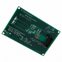
Figure 15. NCP5602 Demo Board http://onsemi.com 11 ...
Page 12
... 0.05 C NOTE 3 *For additional information on our Pb−Free strategy and soldering details, please download the ON Semiconductor Soldering and Mounting Techniques Reference Manual, SOLDERRM/D. N. American Technical Support: 800−282−9855 Toll Free USA/Canada Europe, Middle East and Africa Technical Support: Phone: 421 33 790 2910 Japan Customer Focus Center Phone: 81− ...