NCP5602EVB ON Semiconductor, NCP5602EVB Datasheet - Page 5
NCP5602EVB
Manufacturer Part Number
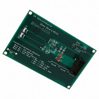
NCP5602EVB
Description
EVAL BOARD FOR NCP5602
Manufacturer
ON Semiconductor
Specifications of NCP5602EVB
Design Resources
NCP5602 EVB BOM NCP5602EVB Gerber Files NCP5602 EVB Schematic
Current - Output / Channel
60mA
Outputs And Type
2, Non-Isolated
Voltage - Output
4.8 ~ 5.7 V
Features
Dimmable
Voltage - Input
3.6V
Utilized Ic / Part
NCP5602
Core Chip
NCP5602
Topology
Charge Pump
No. Of Outputs
2
Development Tool Type
Hardware - Eval/Demo Board
Leaded Process Compatible
Yes
Mcu Supported Families
NCP5602
Rohs Compliant
Yes
Lead Free Status / RoHS Status
Lead free / RoHS Compliant
For Use With/related Products
NCP5602
Other names
NCP5602EVBOS


6. The overall output current tolerance depends upon the accuracy of the external resistor. Using 1% or better resistor is recommended.
7. The external circuit must not force the I
8. Parameter not tested in production, guaranteed by design.
POWER SUPPLY SECTION
temperature, operating conditions 2.85 V < Vbat < 5.5 V, unless otherwise noted.)
ANALOG SECTION
temperature, operating conditions 2.85 V < Vbat < 5.5 V, unless otherwise noted.)
DIGITAL PARAMETERS SECTION
ambient temperature, operating conditions 2.85 V < Vbat < 5.5 V, unless otherwise noted.) Note: Digital inputs undershoot < − 0.30 V to
ground, Digital inputs overshoot < 0.30 V to V
Power Supply
Continuous DC Current in the Load @ Vf = 3.0 V, ICON = L
Output ICON Current (ICON = H) @ T
Continuous Output Short Circuit Current
Output Voltage Compliance (OVP)
DC−DC Start Time (Cout = 1.0 mF) 3.0 V < Vbat = Nominal < 5.5 V
Output Voltage Turn Off Time from Last ACK Bit to Vout = 5%
Standby Current, Vbat = 3.6 V, Iout = 0 mA, ICON = L
Operating Current, @ Iout = 0 mA, ICON = H, Vbat = 3.6 V
Output LED to LED Current Matching, @ 3.0 V < Vbat < 4.2 V,
Output Current Tolerance @ Vbat = 3.6 V, I
Charge Pump Operating Frequency −40°C < Ta < 85°C
Thermal Shutdown Protection
Thermal Shutdown Protection Hysteresis
Efficiency
InputI2C Clock Frequency (Note 8)
Positive Going Input High Voltage Threshold, SCL, SDA Signals
Negative Going Input High Voltage Threshold, SCL, SDA
Reference Current @ Vref = 600 mV (Note 7)
Reference Voltage (Note 7)
Reference Current (IREF) Current Ratio (see Table 2)
@ 3.2 V < Vbat < 5.5 V
@ 3.0 V < Vbat < 5.5 V
Vbat = 3.6 V
from Last ACK Bit to Full Load Operation
@ SCL = SDA = L
@ SCL = SDA = H (No Port Activity)
I
< 85°C
− LED1 = LED2 = 10 mA, Vf = 3.2 V, Vbat = 3.2 V (Total = 20 mA)
− LED1 = LED2 = 30 mA, Vf = 3.4 V, Vbat = 3.75 V (Total = 60 mA)
Signals
LED
one can force to run the normal operation.
= 10 mA, LED1 & LED2 are Identical −25°C < Ta < 85°C
(Typical values are referenced to T
Rating
Rating
Rating
(Typical values are referenced to T
j
REF
= + 25°C, Vf = 2.8 V,
(Typical values are referenced to T
LED
pin voltage either higher or lower than the 600 mV specified. The limits represent the min/max values
BAT
= 10 mA −25°C < Ta
.
http://onsemi.com
A
= +25°C, Min & Max values are referenced −40°C to +85°C ambient
A
5
Pin
Pin
5, 6
5, 6
= +25°C, Min & Max values are referenced −40°C to +85°C ambient
4
4
−
6
2, 3
2, 3
Pin
12
12
11
11
11
7
7
7
7
−
−
−
−
−
A
= +25°C, Min & Max values are referenced −40°C to +85°C
Symbol
Symbol
I
I
F
V
ICONTROL
I
LEDR
Symbol
V
V
REF
SCK
REF
E
Tstart
Fpwr
T
IH
IL
Vout
I
V
Isch
I
I
T
I
Toff
stdb
MAT
TOL
I
PWR
SDH
out
op
SD
bat
−3%
Min
Min
Min
2.7
4.8
1.0
1.3
1.0
60
45
−
−
−
−
−
−
−
−
−
−
−
−
−
−
0
"0.2
"3.0
Typ
Typ
Typ
600
150
300
750
160
600
1.0
45
30
87
84
16
−
−
−
−
−
−
−
−
−
V
Max
Max
+3%
Max
850
150
400
5.5
5.7
6.0
1.0
0.4
12
60
BAT
−
−
−
−
−
−
−
−
−
−
−
−
MHz
Unit
Unit
Unit
kHz
mA
mA
mV
mA
mA
mA
mA
ms
ms
°C
°C
%
%
%
V
V
V
V
−
Related parts for NCP5602EVB
Image
Part Number
Description
Manufacturer
Datasheet
Request
R

Part Number:
Description:
High Efficiency Ultra Small Thinnest White LED Driver
Manufacturer:
ON Semiconductor
Datasheet:
Part Number:
Description:
ON Semiconductor [VOLTAGE REGULATOR]
Manufacturer:
ON Semiconductor
Datasheet:
Part Number:
Description:
357-036-542-201 CARDEDGE 36POS DL .156 BLK LOPRO
Manufacturer:
ON Semiconductor
Datasheet:
Part Number:
Description:
357-036-542-201 CARDEDGE 36POS DL .156 BLK LOPRO
Manufacturer:
ON Semiconductor
Datasheet:
Part Number:
Description:
357-036-542-201 CARDEDGE 36POS DL .156 BLK LOPRO
Manufacturer:
ON Semiconductor
Datasheet:
Part Number:
Description:
357-036-542-201 CARDEDGE 36POS DL .156 BLK LOPRO
Manufacturer:
ON Semiconductor
Datasheet:
Part Number:
Description:
357-036-542-201 CARDEDGE 36POS DL .156 BLK LOPRO
Manufacturer:
ON Semiconductor
Datasheet:
Part Number:
Description:
357-036-542-201 CARDEDGE 36POS DL .156 BLK LOPRO
Manufacturer:
ON Semiconductor
Datasheet:
Part Number:
Description:
357-036-542-201 CARDEDGE 36POS DL .156 BLK LOPRO
Manufacturer:
ON Semiconductor
Datasheet:
Part Number:
Description:
357-036-542-201 CARDEDGE 36POS DL .156 BLK LOPRO
Manufacturer:
ON Semiconductor
Datasheet:
Part Number:
Description:
357-036-542-201 CARDEDGE 36POS DL .156 BLK LOPRO
Manufacturer:
ON Semiconductor
Datasheet:
Part Number:
Description:
357-036-542-201 CARDEDGE 36POS DL .156 BLK LOPRO
Manufacturer:
ON Semiconductor
Datasheet:
Part Number:
Description:
Manufacturer:
ON Semiconductor
Datasheet:
Part Number:
Description:
Manufacturer:
ON Semiconductor
Datasheet: