LM3405XEVAL National Semiconductor, LM3405XEVAL Datasheet - Page 6
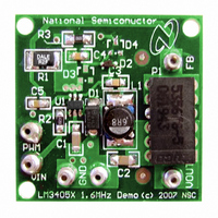
LM3405XEVAL
Manufacturer Part Number
LM3405XEVAL
Description
BOARD EVALUATION LM3405X
Manufacturer
National Semiconductor
Series
PowerWise®r
Specifications of LM3405XEVAL
Current - Output / Channel
1A
Outputs And Type
1, Non-Isolated
Voltage - Output
0.2 ~ 13.5 V
Features
Dimmable
Voltage - Input
3 ~ 15V
Utilized Ic / Part
LM3405
Kit Contents
Board, Datasheet
Svhc
No SVHC (15-Dec-2010)
Kit Features
Cycle-by-Cycle Current Limit,
Rohs Compliant
No
Lead Free Status / RoHS Status
Contains lead / RoHS non-compliant


www.national.com
Block Diagram
Application Information
THEORY OF OPERATION
The LM3405 is a PWM, current-mode control switching buck
regulator designed to provide a simple, high efficiency solu-
tion for driving LEDs with a preset switching frequency of
1.6MHz. This high frequency allows the LM3405 to operate
with small surface mount capacitors and inductors, resulting
in LED drivers that need only a minimum amount of board
space. The LM3405 is internally compensated, simple to use,
and requires few external components.
The following description of operation of the LM3405 will refer
to the Simplified Block Diagram (Figure 1) and to the wave-
forms in Figure 2. The LM3405 supplies a regulated output
current by switching the internal NMOS power switch at con-
stant frequency and variable duty cycle. A switching cycle
begins at the falling edge of the reset pulse generated by the
internal oscillator. When this pulse goes low, the output con-
trol logic turns on the internal NMOS power switch. During this
on-time, the SW pin voltage (V
V
I
ates an output proportional to the switch current. The sense
signal is summed with the regulator’s corrective ramp and
compared to the error amplifier’s output, which is proportional
to the difference between the feedback voltage and V
When the PWM comparator output goes high, the internal
power switch turns off until the next switching cycle begins.
During the switch off-time, inductor current discharges
through the catch diode D1, which forces the SW pin to swing
below ground by the forward voltage (V
The regulator loop adjusts the duty cycle (D) to maintain a
constant output current (I
pin voltage to be equal to V
L
IN
is measured by the current sense amplifier, which gener-
, and the inductor current (I
F
) through the LED, by forcing FB
REF
SW
L
) increases with a linear slope.
(0.205V).
) swings up to approximately
D1
) of the catch diode.
FIGURE 1. Simplified Block Diagram
REF
.
6
BOOST FUNCTION
Capacitor C3 and diode D2 in Figure 1 are used to generate
a voltage V
the gate drive voltage to the internal NMOS power switch. To
properly drive the internal NMOS switch during its on-time,
V
value of V
ficiency by minimizing both the internal switch ON resistance
(R
V
of 5.5V.
BOOST
BOOST
DS(ON)
FIGURE 2. SW Pin Voltage and Inductor Current
- V
needs to be at least 2.5V greater than V
), and the switch rise and fall times. However,
BOOST
SW
BOOST
should not exceed the maximum operating limit
- V
. The voltage across C3, V
Waveforms of LM3405
SW
is recommended to achieve better ef-
BOOST
SW
20178907
- V
20178906
. Large
SW
, is
Related parts for LM3405XEVAL
Image
Part Number
Description
Manufacturer
Datasheet
Request
R

Part Number:
Description:
Precision Fahrenheit Temperature Sensors
Manufacturer:
National Semiconductor
Part Number:
Description:
National Semiconductor [8-Bit D/A Converter]
Manufacturer:
National Semiconductor
Datasheet:
Part Number:
Description:
National Semiconductor [Media Coprocessor]
Manufacturer:
National Semiconductor
Datasheet:
Part Number:
Description:
Digitally Controlled Tone and Volume Circuit with Stereo Audio Power Amplifier, Microphone Preamp Stage and National 3D Sound
Manufacturer:
National Semiconductor
Datasheet:
Part Number:
Description:
Digitally Controlled Tone and Volume Circuit with Stereo Audio Power Amplifier, Microphone Preamp Stage and National 3D Sound
Manufacturer:
National Semiconductor
Datasheet:
Part Number:
Description:
AC97 Rev 2 Codec with Sample Rate Conversion and National 3D Sound
Manufacturer:
National Semiconductor
Part Number:
Description:
Manufacturer:
National Semiconductor
Datasheet:
Part Number:
Description:
Manufacturer:
National Semiconductor
Datasheet:
Part Number:
Description:
General Purpose, Low Voltage, Low Power, Rail-to-Rail Output Operational Amplifiers
Manufacturer:
National Semiconductor
Datasheet:
Part Number:
Description:
8-bit 20 MSPS flash A/D converter.
Manufacturer:
National Semiconductor
Datasheet:
Part Number:
Description:
Low Noise Quad Operational Amplifier
Manufacturer:
National Semiconductor
Datasheet:
Part Number:
Description:
Quad Differential Line Receivers
Manufacturer:
National Semiconductor
Datasheet:
Part Number:
Description:
Quad High Speed Trapezoidal? Bus Transceiver
Manufacturer:
National Semiconductor
Datasheet: