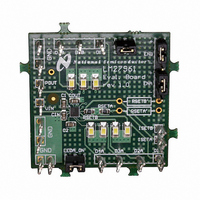
LM27961TLEV National Semiconductor, LM27961TLEV Datasheet

LM27961TLEV
Specifications of LM27961TLEV
Related parts for LM27961TLEV
LM27961TLEV Summary of contents
Page 1
... The LM27961 is available in National’s chip-scale 18-bump micro SMD package. Typical Application Circuit © 2004 National Semiconductor Corporation Features n Drives 4 Individual Common-Anode LEDs with up to 20mA each for a Main Display Backlight n Drives 3 Individual Common-Cathode LEDs with up to ...
Page 2
Connection Diagram Pin Description Pin #s Pin Names GND A3 P OUT A1, B2, A5, E1 C1+, C1-, C2+, C2- D6, E5, D4, E3 D1A, D2A, D3A, D4A C5, B4, C3 D1B, D2B, D3B B6 EN-A ...
Page 3
... Absolute Maximum Ratings If Military/Aerospace specified devices are required, please contact the National Semiconductor Sales Office/ Distributors for availability and specifications. V pin voltage IN ENA, ENB pin voltages I Pin Voltages Dxx Continuous Power Dissipation (Note 3) Junction Temperature (T ) J-MAX Storage Temperature Range Maximum Lead Temperature (Soldering, 10 sec ...
Page 4
Electrical Characteristics Limits in standard typeface are for T less otherwise specified 3.6V 1.5V 8.35kΩ; C SETA SETB IN pins (I and I ) apply to both Group A and Group B. ...
Page 5
Typical Performance Characteristics = 3.6V; ENA = V and ENB = GND, or ENA = GND and ENB = V IN 1µF. LED Current (D1A, D2A,D3A, D4A) vs. Input Voltage Quiescent Current vs. Input Voltage, Unless otherwise specified ...
Page 6
Typical Performance Characteristics = 3.6V; ENA = V and ENB = GND, or ENA = GND and ENB = V IN 1µF. (Continued) Charge Pump Output Voltage vs. Output Current Input Current vs. Input Voltage www.national.com Unless otherwise specified: V ...
Page 7
Typical Performance Characteristics = 3.6V; ENA = V and ENB = GND, or ENA = GND and ENB = V IN 1µF. (Continued) Charge Pump Switching Frequency vs. Input Voltage Diode Current (DxB) vs. Headroom Voltage (DxB) Unless otherwise specified: ...
Page 8
Typical Performance Characteristics = 3.6V; ENA = V and ENB = GND, or ENA = GND and ENB = V IN 1µF. (Continued) Diode Current (DxA) vs. R SETx ENx Signal (Top) and Charge Pump Start-Up (Bottom) Waveforms Vertical Scale ...
Page 9
Block Diagram Circuit Description OVERVIEW The LM27961 is primarily intended for Lithium-Ion battery driven white-LED drive applications, and is well suited to drive white LEDs that are used for backlighting small-format displays. The part has seven matched constant-current out- puts, ...
Page 10
Circuit Description (Continued) anode outputs and a group of 3 common cathode outputs. There is an ON/OFF control pin for each group (ENA and ENB). The DC current through the LEDs is programmed with an external resistor. Changing currents on-the-fly ...
Page 11
Circuit Description (Continued) FIGURE 2. One Parallel Connected LED Connecting outputs in parallel does not affect internal opera- tion of the LM27961 and has no impact on the Electrical Characteristics and limits previously presented. The avail- able diode output current, ...
Page 12
Applications Information The voltage rating of the output capacitor should be 10V or more. All other capacitors should have a voltage rating at or above the maximum input voltage of the application. CIRCUIT BOARD LAYOUT For optimal, low-noise performance, all ...
Page 13
... BANNED SUBSTANCE COMPLIANCE National Semiconductor certifies that the products and packing materials meet the provisions of the Customer Products Stewardship Specification (CSP-9-111C2) and the Banned Substances and Materials of Interest Specification (CSP-9-111S2) and contain no ‘‘Banned Substances’’ as defined in CSP-9-111S2. ...


