NCP5603GEVB ON Semiconductor, NCP5603GEVB Datasheet - Page 4
NCP5603GEVB
Manufacturer Part Number
NCP5603GEVB
Description
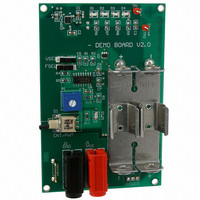
EVAL BOARD FOR NCP5603G HI FREQ
Manufacturer
ON Semiconductor
Specifications of NCP5603GEVB
Design Resources
NCP5603 EVB BOM NCP5603GEVB Gerber Files NCP5603 EVB Schematic
Current - Output / Channel
160mA
Outputs And Type
1, Non-Isolated
Voltage - Output
4.5 ~ 5 V
Features
Dimmable
Voltage - Input
3V or 3.6V
Utilized Ic / Part
NCP5603
Core Chip
NCP5603
Topology
Charge Pump
No. Of Outputs
1
Development Tool Type
Hardware - Eval/Demo Board
Leaded Process Compatible
Yes
Mcu Supported Families
NCP5603
Rohs Compliant
Yes
Lead Free Status / RoHS Status
Lead free / RoHS Compliant
For Use With/related Products
NCP5603G
Other names
NCP5603GEVBOS


1. Using ceramic 16 V working voltage capacitors is recommended to compensate the DC bias effect encountered with such type of capacitors.
2. Any external impedance connected to pin 6 shall be 10 kW or higher.
PIN FUNCTION DESCRIPTION
Pin
10
1
2
3
4
5
6
7
8
9
EN/PWM
Symbol
GND
C1N
Vsel
C2N
C1P
C2P
V
Fsel
V
out
bat
OUTPUT, PWR
INPUT, Digital
INPUT, Digital
INPUT, Digital
GROUND
POWER
POWER
POWER
POWER
POWER
Type
This pin supplies the regulated voltage to the external LED. Since high current transients
are present in this pin, care must be observed to avoid voltage spikes in the system. Good
high frequency layout technique must be observed.
One side of the external charge pump capacitor (C
with C1P, pin 9. Using low ESR ceramic capacitor is recommended to optimize the Charge
Pump efficiency.
This pin shall be connected to the power source, and must be decoupled to Ground by a
low ESR capacitor (2.2 mF/6.3 V ceramic or better (see Note 1)).
This pin is used to program the operating frequency:
This pin setup the output voltage:
This pin controls the activity of the NCP5603 chip:
The NCP5603 can operate either in a continuous mode (EN/PWM = High), or can be
controlled by a PWM pulse applied to EN/PWM to dim the output light. When EN/PWM is
Low, the external load is disconnected from the converter, providing a very low standby
current. The pull down built-in resistance makes sure the chip is deactivated even if the
EN/PWM pin is disconnected (see Note 2).
One side of the external charge pump capacitor (C
with C2P, pin 10. Using low ESR ceramic capacitor is recommended to optimize the
Charge Pump efficiency.
This pin combines the Signal ground and the Power ground and must be connected to the
system ground. Using good quality ground plane is mandatory to avoid spikes on the logic
signal lines.
One side of the external charge pump capacitor (C
with C1N, pin 2. Using low ESR ceramic capacitor is recommended to optimize the Charge
Pump efficiency.
One side of the external charge pump capacitor is connected to this pin, associated with
C2N, pin 7. Using low ESR ceramic capacitor is recommended to optimize the Charge
Pump efficiency.
Fsel = 0 → Fop = 262 kHz
Fsel = 1 → Fop = 650 kHz
Vsel = 0 → V
Vsel = 1 → V
EN/PWM = Low → the chip is deactivated, the load is disconnected
EN/PWM = High → the chip is activated and the load is connected to the
http://onsemi.com
regulated output current.
out
out
NCP5603
= 4.5 V
= 5.0 V
4
Description
FLY
FLY
FLY
) is connected to this pin, associated
) is connected to this pin, associated
) is connected to this pin, associated
Related parts for NCP5603GEVB
Image
Part Number
Description
Manufacturer
Datasheet
Request
R

Part Number:
Description:
High Efficiency Charge Pump Converter
Manufacturer:
ON Semiconductor
Datasheet:
Part Number:
Description:
ON Semiconductor [VOLTAGE REGULATOR]
Manufacturer:
ON Semiconductor
Datasheet:
Part Number:
Description:
357-036-542-201 CARDEDGE 36POS DL .156 BLK LOPRO
Manufacturer:
ON Semiconductor
Datasheet:
Part Number:
Description:
357-036-542-201 CARDEDGE 36POS DL .156 BLK LOPRO
Manufacturer:
ON Semiconductor
Datasheet:
Part Number:
Description:
357-036-542-201 CARDEDGE 36POS DL .156 BLK LOPRO
Manufacturer:
ON Semiconductor
Datasheet:
Part Number:
Description:
357-036-542-201 CARDEDGE 36POS DL .156 BLK LOPRO
Manufacturer:
ON Semiconductor
Datasheet:
Part Number:
Description:
357-036-542-201 CARDEDGE 36POS DL .156 BLK LOPRO
Manufacturer:
ON Semiconductor
Datasheet:
Part Number:
Description:
357-036-542-201 CARDEDGE 36POS DL .156 BLK LOPRO
Manufacturer:
ON Semiconductor
Datasheet:
Part Number:
Description:
357-036-542-201 CARDEDGE 36POS DL .156 BLK LOPRO
Manufacturer:
ON Semiconductor
Datasheet:
Part Number:
Description:
357-036-542-201 CARDEDGE 36POS DL .156 BLK LOPRO
Manufacturer:
ON Semiconductor
Datasheet:
Part Number:
Description:
357-036-542-201 CARDEDGE 36POS DL .156 BLK LOPRO
Manufacturer:
ON Semiconductor
Datasheet:
Part Number:
Description:
357-036-542-201 CARDEDGE 36POS DL .156 BLK LOPRO
Manufacturer:
ON Semiconductor
Datasheet:
Part Number:
Description:
Manufacturer:
ON Semiconductor
Datasheet:
Part Number:
Description:
Manufacturer:
ON Semiconductor
Datasheet: