NCP5603GEVB ON Semiconductor, NCP5603GEVB Datasheet - Page 6
NCP5603GEVB
Manufacturer Part Number
NCP5603GEVB
Description
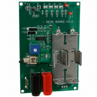
EVAL BOARD FOR NCP5603G HI FREQ
Manufacturer
ON Semiconductor
Specifications of NCP5603GEVB
Design Resources
NCP5603 EVB BOM NCP5603GEVB Gerber Files NCP5603 EVB Schematic
Current - Output / Channel
160mA
Outputs And Type
1, Non-Isolated
Voltage - Output
4.5 ~ 5 V
Features
Dimmable
Voltage - Input
3V or 3.6V
Utilized Ic / Part
NCP5603
Core Chip
NCP5603
Topology
Charge Pump
No. Of Outputs
1
Development Tool Type
Hardware - Eval/Demo Board
Leaded Process Compatible
Yes
Mcu Supported Families
NCP5603
Rohs Compliant
Yes
Lead Free Status / RoHS Status
Lead free / RoHS Compliant
For Use With/related Products
NCP5603G
Other names
NCP5603GEVBOS


5. Temperature range guaranteed by design, not production tested.
6. Smaller footprint associated to lower working voltages (10 V or 6.3 V, size 0805 or 0602) can be used, but care must be observed to prevent
7. Ceramic X7R, ESR < 100 mW, SMD type capacitors are mandatory to achieve the I
8. Digital inputs undershoot < - 0.30 V to ground, Digital inputs overshoot < 0.30 V to V
ELECTRICAL CHARACTERISTICS
Power Supply
Quiescent Current @ V
Shutdown Current @ I
Output Voltage Regulation
Continuous DC Load Current (Note 7)
Cin = 1.0 mF, C
Pulsed Output Current
Cin = 10 mF, C
Output Continuous Short Circuit Current, V
Operating Frequency (Note 5)
Output Voltage Ripple (Note 6)
Fop = 262 kHz, I
Digital Input High Level
Digital Input Low level
Output Power Efficiency
Thermal Shut Down Protection
Hysteresis
DC bias effect on the capacitance final value. See capacitor manufacturer data sheets.
might be necessary to use two 2.2 mF/6.3 V/ceramic capacitors in parallel, yielding an improved V
the other hand, care must be observed to take into account the DC bias impact on the capacitance value. See ceramic capacitor manufacturer
data sheets.
@ Pulsed Clock Fop = 262 kHz
@ Pulsed Clock Fop = 650 kHz
@ Continuous Clock Fop = 262 kHz
@ Continuous Clock Fop = 650 kHz
@ 2.85 < V
@ V
@ Vsel = 1, 2.85 V < V
@ Vsel = 0, 2.85 V < V
@ Vsel = 1, 3.2 V < V
@ Vsel = 0, 3.2 V < V
@ Vsel = 1, 2.85 V < V
@ Vsel = 0, 2.85 V < V
@ Fsel = 0, 2.85 V < V
@ Fsel = 1, 2.85 V < V
@ C
@ C
@ V
@ V
bat
out
out
bat
bat
= 5.5 V
= 3.3 V, V
= 3.9 V, V
= 1.0 mF
= 4.7 mF
Pwidth = 500 ms, -40°C < T
bat
FLY
FLY
out
< 4.2 V
= 1.0 mF, Cout = 10 mF, V
= 1.0 mF, Cout = 1.0 mF
out
out
= 60 mA (Note 7)
out
= 5.0 V, I
= 5.0 V, I
Characteristic
bat
bat
bat
bat
bat
bat
bat
bat
bat
= 0 mA, EN/PWM = L
= 3.7 V, I
< 4.3 V
< 4.3 V
< 4.5 V
< 4.5 V
< 4.3 V
< 4.3 V
< 4.3 V
< 4.3 V
out
out
= 60 mA, Fop = 262 kHz
= 160 mA, Fop = 650 kHz
out
A
= 0 mA
< +65°C
@ 2.85 V < Vbat < 5.5 V (-40°C to +85°C ambient temperature, unless otherwise noted).
out
bat
= 0 V
= 3.6 V
http://onsemi.com
NCP5603
4, 5, 6
4, 5, 6
Pin
6
3
3
3
3
3
3
3
3
Symbol
T
V
Iqsc
I
I
Isch
V
Fop
V
I
V
stdb
FLH
V
Ph
HSD
out
bat
out
PP
IH
IL
out
bat
specifications. Depending upon the PCB layout, it
.
4.275
2.85
4.75
Min
210
500
1.3
-
-
-
-
-
-
-
-
-
-
-
-
-
-
-
-
-
-
-
out
noise over the temperature range. On
Typ
350
262
650
150
160
1.0
2.1
5.0
4.5
40
25
75
84
20
-
-
-
-
-
-
-
-
-
-
-
4.725
1000
Max
5.25
160
200
120
100
320
5.5
0.8
1.2
2.5
4.0
0.4
80
60
-
-
-
-
-
-
-
-
-
Unit
kHz
mA
mA
mA
mA
mV
mA
°C
%
V
V
V
V
Related parts for NCP5603GEVB
Image
Part Number
Description
Manufacturer
Datasheet
Request
R

Part Number:
Description:
High Efficiency Charge Pump Converter
Manufacturer:
ON Semiconductor
Datasheet:
Part Number:
Description:
ON Semiconductor [VOLTAGE REGULATOR]
Manufacturer:
ON Semiconductor
Datasheet:
Part Number:
Description:
357-036-542-201 CARDEDGE 36POS DL .156 BLK LOPRO
Manufacturer:
ON Semiconductor
Datasheet:
Part Number:
Description:
357-036-542-201 CARDEDGE 36POS DL .156 BLK LOPRO
Manufacturer:
ON Semiconductor
Datasheet:
Part Number:
Description:
357-036-542-201 CARDEDGE 36POS DL .156 BLK LOPRO
Manufacturer:
ON Semiconductor
Datasheet:
Part Number:
Description:
357-036-542-201 CARDEDGE 36POS DL .156 BLK LOPRO
Manufacturer:
ON Semiconductor
Datasheet:
Part Number:
Description:
357-036-542-201 CARDEDGE 36POS DL .156 BLK LOPRO
Manufacturer:
ON Semiconductor
Datasheet:
Part Number:
Description:
357-036-542-201 CARDEDGE 36POS DL .156 BLK LOPRO
Manufacturer:
ON Semiconductor
Datasheet:
Part Number:
Description:
357-036-542-201 CARDEDGE 36POS DL .156 BLK LOPRO
Manufacturer:
ON Semiconductor
Datasheet:
Part Number:
Description:
357-036-542-201 CARDEDGE 36POS DL .156 BLK LOPRO
Manufacturer:
ON Semiconductor
Datasheet:
Part Number:
Description:
357-036-542-201 CARDEDGE 36POS DL .156 BLK LOPRO
Manufacturer:
ON Semiconductor
Datasheet:
Part Number:
Description:
357-036-542-201 CARDEDGE 36POS DL .156 BLK LOPRO
Manufacturer:
ON Semiconductor
Datasheet:
Part Number:
Description:
Manufacturer:
ON Semiconductor
Datasheet:
Part Number:
Description:
Manufacturer:
ON Semiconductor
Datasheet: