AD8330-EVALZ Analog Devices Inc, AD8330-EVALZ Datasheet - Page 20
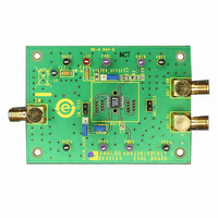
AD8330-EVALZ
Manufacturer Part Number
AD8330-EVALZ
Description
BOARD EVAL FOR AD8330
Manufacturer
Analog Devices Inc
Specifications of AD8330-EVALZ
Channels Per Ic
1 - Single
Amplifier Type
Variable Gain
Output Type
Differential, Rail-to-Rail
Slew Rate
1500 V/µs
-3db Bandwidth
150MHz
Operating Temperature
-40°C ~ 85°C
Current - Supply (main Ic)
20mA
Voltage - Supply, Single/dual (±)
2.7 V ~ 6 V
Board Type
Fully Populated
Utilized Ic / Part
AD8330
Silicon Manufacturer
Analog Devices
Application Sub Type
Variable Gain Amplifier
Kit Application Type
Amplifier
Silicon Core Number
AD8330
Kit Contents
Board
Lead Free Status / RoHS Status
Lead free / RoHS Compliant
Current - Output / Channel
-
Lead Free Status / RoHS Status
Lead free / RoHS Compliant, Lead free / RoHS Compliant


AD8330
The gain calibration is specified for an open-circuited load,
such as the high input resistance of an ADC. When resistively
loaded, all gain values are nominally lowered as follows:
Thus, when R
R
Gain Errors Due to On-Chip Resistor Tolerances
In all cases where external resistors are used, keep in mind that
all on-chip resistances, including the R
(R
These variances need to be accounted for when calculating the
gain with input and output loading. This sensitivity can be avoided
by adjusting the source and load resistances to bear an inverse
relationship as follows:
The simplest case is when R
the gain is 12 dB lower than the basic value. The reduction of
peak swing at the load can be corrected by using V
thereby restoring 6 dB of gain; using V
basic gain and doubles the peak available output swing.
Output (Input) Common-Mode Control
The output voltages are nominally positioned at the midpoint of
the supply, V
appears at Pin CNTR, which is not normally expected to be
loaded (the source resistance is ~4 kΩ). However, some circum-
stances require a small change in this voltage, and a resistor
from CNTR to ground can lower this voltage, whereas a resistor
to the supply raises it. On the other hand, this pin can be driven
by an external voltage source to set the common-mode level to
satisfy, for example, the needs of a following ADC. Any value
from 0.5 V above ground to 0.5 V below the supply is permissible.
Of course, when using an extreme common-mode level, the
available output swing is limited, and it is recommended that
a value equal or close to the default of V
There may be a few millivolts of offset between the applied
voltage and the actual common-mode level at the output pins.
The input common-mode voltage, V
Pin INLO is slaved to the output, but with a shifted value of
for V
when V
USING THE AD8330
This section describes a few general aspects of using the
AD8330. Applying the AD8330 to a wide variety of circum-
stances requires very few precautions.
L
I
= 75 Ω, the reduction is 9.5 dB; and for R
), are subject to variances of up to ±20%.
If R
if R
V
G
DBS
CMI
LOADED
S
L
S
= 0.75 and T = 25°C. Thus, the default value for V
= 5 V is 3.01 V (see Figure 55).
= αR
= αR
= 0.757 V
S
/2, over the range 2.7 V < V
L
=
I
O
, then make R
= 150 Ω, the gain is reduced by 6 dB; for
, then make R
G
(
150
UNLOADED
CNTR
Ω
+
+ 1.12 V
R
R
L
S
L
)
L
= 1 kΩ and R
S
= R
= R
O
I
/α
/α; or,
CMI
O
MAG
, at Pin INHI and
CNTR
and the input resistance
S
= 2 V restores the full
L
< 6 V, and this voltage
= 150 Ω, therefore,
L
= V
= 50 Ω, it is 12 dB.
S
/2 be used.
MAG
= 1 V,
CMI
(13)
(14)
Rev. E | Page 20 of 32
As in all high frequency circuits, careful observation of the
ground nodes associated with each function is important. Three
positive supply pins are provided: VPSI supports the input cir-
cuitry that often operates at a relatively high sensitivity; VPOS
supports general bias sources and needs no decoupling; and
VPSO biases the output stage where decoupling can be useful in
maintaining a glitch-free output. Figure 57 shows the general
case, where VPSI and VPSO are each provided with their own
decoupling network, but this is not needed in all cases.
Because of the differential nature of the signal path, power
supply decoupling is, in general, much less critical than in a
single-sided amplifier; and where the minimization of board-
level components is especially crucial, it is possible that these
pins need no decoupling at all. On the other hand, when the
signal source is single-sided, giving extra attention to the
decoupling on Pin VPSI is sometimes required. Likewise,
care is required in decoupling the VPSO pin if the output is
loaded on only one of its two output pins. The general common
(COMM) and the output stage common (CMOP) are usually
grounded as shown in the Figure 57; however, the Applications
section shows how a negative supply can optionally be used.
The AD8330 is enabled by taking the ENBL pin to a logical high
(or, in all cases, the supply). The UP gain mode is enabled either
by leaving the MODE pin unconnected or taking it to a logical
high. When the opposite gain direction is needed, the MODE
pin should be grounded or driven to a logical low. The low-pass
corner of the offset loop is determined by Capacitor CHPF; this
is preferably tied to the CNTR pin that in turn, should be
decoupled to ground. The gain interface common pin (CMGN)
is grounded, and the output magnitude control pin (VMAG) is
left unconnected, or can optionally be connected to a 500 mV
source for basic gain calibration.
INPUT,
0V TO ±2V MAX
BASIC GAIN BIAS
V
DBS :
CD1
R
D
0V TO 1.5V
1
Figure 57. Power Supply Decoupling and Basic Connections
NC
VPSI
INHI
INLO
MODE
E
VDBS
N
B
L
VGA CORE
BIAS AND
GAIN INTERFACE
V-REF
OFST
CMGN
C
H
P
OFFSET CONTROL
F
CM MODE AND
VPOS
COMM
OUTPUT
STAGES
CONTROL
OUTPUT
V
S
C
VMAG
NC
2.7V TO 6V
N
VPSO
OPHI
OPLO
CMOP
CD2
GROUND
T
R
OUTPUT,
±2V MAX
CD3
RD2
Related parts for AD8330-EVALZ
Image
Part Number
Description
Manufacturer
Datasheet
Request
R

Part Number:
Description:
BOARD EVAL FOR AD8330
Manufacturer:
Analog Devices Inc
Datasheet:

Part Number:
Description:
±1.7g Dual-Axis IMEMS Accelerometer Evaluation Board
Manufacturer:
Analog Devices Inc
Datasheet:

Part Number:
Description:
Inertial Sensor Evaluation System
Manufacturer:
Analog Devices Inc
Datasheet:
Part Number:
Description:
Manufacturer:
Analog Devices Inc
Datasheet:
Part Number:
Description:
Manufacturer:
Analog Devices Inc
Datasheet:
Part Number:
Description:
Manufacturer:
Analog Devices Inc
Datasheet:
Part Number:
Description:
Manufacturer:
Analog Devices Inc
Datasheet:
Part Number:
Description:
Manufacturer:
Analog Devices Inc
Datasheet:
Part Number:
Description:
Manufacturer:
Analog Devices Inc
Datasheet:
Part Number:
Description:
Manufacturer:
Analog Devices Inc
Datasheet:
Part Number:
Description:
Manufacturer:
Analog Devices Inc
Datasheet:
Part Number:
Description:
Manufacturer:
Analog Devices Inc
Datasheet:
Part Number:
Description:
Manufacturer:
Analog Devices Inc
Datasheet: