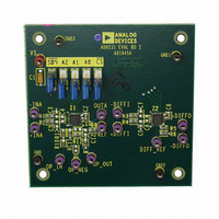
AD8231-EVALZ Analog Devices Inc, AD8231-EVALZ Datasheet - Page 18
AD8231-EVALZ
Manufacturer Part Number
AD8231-EVALZ
Description
BOARD EVAL FOR AD8231
Manufacturer
Analog Devices Inc
Specifications of AD8231-EVALZ
Channels Per Ic
2 - Dual
Amplifier Type
Instrumentation
Output Type
Single-Ended
Slew Rate
1.1 V/µs
Current - Output / Channel
70mA
Operating Temperature
-40°C ~ 125°C
Current - Supply (main Ic)
4mA
Voltage - Supply, Single/dual (±)
3 V ~ 6 V, ±1.5 V ~ 3 V
Board Type
Fully Populated
Utilized Ic / Part
AD8231
Silicon Manufacturer
Analog Devices
Application Sub Type
Instrumentation Amplifier
Kit Application Type
Amplifier
Silicon Core Number
AD8231
Kit Contents
Board
Lead Free Status / RoHS Status
Lead free / RoHS Compliant
-3db Bandwidth
-
Lead Free Status / RoHS Status
Lead free / RoHS Compliant, Lead free / RoHS Compliant
Available stocks
Company
Part Number
Manufacturer
Quantity
Price
Company:

Part Number:
AD8231-EVALZ
Manufacturer:
Analog Devices Inc
Quantity:
135


AD8231
THEORY OF OPERATION
AMPLIFIER ARCHITECTURE
The AD8231 is based on the classic 3-op amp topology. This
topology has two stages: a preamplifier to provide amplification,
followed by a difference amplifier to remove the common-mode
voltage. Figure 49 shows a simplified schematic of the AD8231.
The preamp stage is composed of Amplifier A1, Amplifier A2,
and a digitally controlled resistor network. The second stage is a
gain of 1 difference amplifier composed of Amplifier A3 and
four 14 kΩ resistors. A1, A2, and A3 are all zero drift, rail-to-
rail input, rail-to rail-output amplifiers.
The AD8231 design makes it extremely robust over temperature.
The AD8231 uses an internal thin film resistor to set the gain.
Because all of the resistors are on the same die, gain temperature
drift performance and CMRR drift performance are better than
can be achieved with topologies using external resistors. The
AD8231 also uses an auto-zero topology to null the offsets of all its
internal amplifiers. Because this topology continually corrects for
any offset errors, offset temperature drift is nearly nonexistent.
The AD8231 also includes a free operational amplifier. Like
the other amplifiers in the AD8231, it is a zero drift, rail-to-rail
input, rail-to-rail output architecture.
GAIN SELECTION
The gain of the AD8231 is set by voltages applied to the A0, A1,
and A2 pins. To change the gain, the CS pin must be driven
low. When the CS pin is driven high, the gain is latched, and
voltages at the A0 to A2 pins have no effect. Because the CS pin
is level sensitive rather than edge sensitive, it can also be tied
permanently low. Table 7 shows the different gain settings.
The time required for a gain change is dominated by the settling
time of the amplifier. The AD8231 takes about 200 ns to switch
gains, after which the amplifier begins to settle. Refer to Figure 28
through Figure 32 to determine the settling time for different gains.
–INA
+INA
A1
A2
+V
S
CS
Figure 49. Simplified Schematic
A0
14kΩ
14kΩ
Rev. A | Page 18 of 24
A1
–V
S
A2
A3
14kΩ
14kΩ
Table 7. Truth Table for AD8231 Gain Settings
CS
Low
Low
Low
Low
Low
Low
Low
Low
High
REFERENCE TERMINAL
The output voltage of the AD8231 is developed with respect to
the potential on the reference terminal, which is useful when
the output signal needs to be offset to a midsupply level. For
example, a voltage source can be tied to the REF pin to level-
shift the output so that the AD8231 can drive a single-supply
ADC. The REF pin is protected with ESD diodes and should
not exceed either +V
For best performance, source impedance to the REF terminal
should be kept below 1 Ω. As shown in Figure 49, the reference
terminal, REF, is at one end of a 14 kΩ resistor. Additional
impedance at the REF terminal adds to this 14 kΩ resistor
and results in amplification of the signal connected to the
positive input, causing a CMRR error.
REF
AD8231
V
REF
A2
Low
Low
Low
Low
High
High
High
High
X
INCORRECT
SDN
A4
AD8231
+
–
IN-AMP
Figure 50. Driving the Reference (REF)
REF
S
A1
Low
Low
High
High
Low
Low
High
High
X
or −V
OUTB
–INB
+INB
OUTA
S
by more than 0.3 V.
V
REF
A0
Low
High
Low
High
Low
High
Low
High
X
AD8231
+
–
OP AMP
CORRECT
AD8231
+
–
Gain
1
2
4
8
16
32
64
128
No change
IN-AMP
REF
Related parts for AD8231-EVALZ
Image
Part Number
Description
Manufacturer
Datasheet
Request
R

Part Number:
Description:
Dual, 16 MHz, Rail-to-Rail FET Input Amplifier
Manufacturer:
Analog Devices
Datasheet:

Part Number:
Description:
±1.7g Dual-Axis IMEMS Accelerometer Evaluation Board
Manufacturer:
Analog Devices Inc
Datasheet:

Part Number:
Description:
Inertial Sensor Evaluation System
Manufacturer:
Analog Devices Inc
Datasheet:
Part Number:
Description:
Manufacturer:
Analog Devices Inc
Datasheet:
Part Number:
Description:
Manufacturer:
Analog Devices Inc
Datasheet:
Part Number:
Description:
Manufacturer:
Analog Devices Inc
Datasheet:
Part Number:
Description:
Manufacturer:
Analog Devices Inc
Datasheet:
Part Number:
Description:
Manufacturer:
Analog Devices Inc
Datasheet:
Part Number:
Description:
Manufacturer:
Analog Devices Inc
Datasheet:
Part Number:
Description:
Manufacturer:
Analog Devices Inc
Datasheet:
Part Number:
Description:
Manufacturer:
Analog Devices Inc
Datasheet:
Part Number:
Description:
Manufacturer:
Analog Devices Inc
Datasheet:
Part Number:
Description:
Manufacturer:
Analog Devices Inc
Datasheet: