AD8224-EVALZ Analog Devices Inc, AD8224-EVALZ Datasheet - Page 20
AD8224-EVALZ
Manufacturer Part Number
AD8224-EVALZ
Description
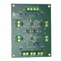
BOARD EVALUATION AD8224
Manufacturer
Analog Devices Inc
Specifications of AD8224-EVALZ
Channels Per Ic
2 - Dual
Amplifier Type
Instrumentation
Output Type
Single-Ended, Rail-to-Rail
Slew Rate
2 V/µs
-3db Bandwidth
1.5MHz
Current - Output / Channel
15mA
Operating Temperature
-40°C ~ 85°C
Current - Supply (main Ic)
750µA
Voltage - Supply, Single/dual (±)
4.5 V ~ 36 V, ±2.25 V ~ 18 V
Board Type
Fully Populated
Utilized Ic / Part
AD8224
Silicon Manufacturer
Analog Devices
Application Sub Type
JFET Input Instrumentation Amplifier
Kit Application Type
Amplifier
Silicon Core Number
AD8224
Kit Contents
Board
Lead Free Status / RoHS Status
Lead free / RoHS Compliant
Available stocks
Company
Part Number
Manufacturer
Quantity
Price
Company:

Part Number:
AD8224-EVALZ
Manufacturer:
Analog Devices Inc
Quantity:
135


AD8224
THEORY OF OPERATION
The AD8224 is a JFET input, monolithic instrumentation amplifier
based on the classic three op amp topology (see Figure 55). Input
Transistor J1 and Input Transistor J2 are biased at a fixed current so
that any input signal forces the output voltages of A1 and A2 to
change accordingly. The input signal creates a current through R
that flows in R1 and R2 such that the outputs of A1 and A2 provide
the correct, gained signal. Topologically, J1, A1, and R1 and J2, A2,
and R2 can be viewed as precision current feedback amplifiers with
a gain bandwidth of 1.5 MHz. The common-mode voltage and
amplified differential signal from A1 and A2 are applied to a
difference amplifier that rejects the common-mode voltage but
amplifies the differential signal. The difference amplifier employs
20 kΩ laser trimmed resistors that result in an in-amp with a gain
error of less than 0.04%. New trim techniques were developed to
ensure that the CMRR exceeds 86 dB (G = 1).
Using JFET transistors, the AD8224 offers an extremely high
input impedance, extremely low bias currents of 10 pA maximum,
low offset current of 0.6 pA maximum, and no input bias
current noise. In addition, input offset is less than 175 μV
and drift is less than 5 μV/°C. Ease of use and robustness were
considered. A common problem for instrumentation amplifiers
is that at high gains, when the input is overdriven, an excessive
milliampere input bias current can result, and the output can
undergo phase reversal.
Overdriving the input at high gains refers to when the input
signal is within the supply voltages but the amplifier cannot
output the gained signal. For example, at a gain of 100, driving
the amplifier with 10 V on ±15 V constitutes overdriving the
inputs because the amplifier cannot output 100 V.
+IN
+V
–V
S
S
+V
J1
S
V
PINCH
I
Q1
C1
24.7kΩ
NODE A
R1
A1
+V
NODE C
–V
S
S
–V
R
G
S
VB
NODE D
Figure 55. Simplified Schematic
+V
–V
S
S
NODE B
Rev. B | Page 20 of 28
A2
G
R2
24.7kΩ
C2
The AD8224 has none of these problems; its input bias current
is limited to less than 10 μA, and the output does not phase
reverse under overdrive fault conditions.
The AD8224 has extremely low load induced nonlinearity. All
amplifiers that comprise the AD8224 have rail-to-rail output
capability for enhanced dynamic range. The input of the AD8224
can amplify signals with wide common-mode voltages even
slightly lower than the negative supply rail. The AD8224 operates
over a wide supply voltage range. It can operate from either a
single +4.5 V to +36 V supply or a dual ±2.25 V to ±18 V. The
transfer function of the AD8224 is
Users can easily and accurately set the gain using a single,
standard resistor. Because the input amplifiers employ a current
feedback architecture, the AD8224 gain bandwidth product
increases with gain, resulting in a system that does not experience
as much bandwidth loss as voltage feedback architectures at
higher gains.
GAIN SELECTION
Placing a resistor across the R
AD8224. This is calculated by referring to Table 12 or by using
the following gain equation
Q2
V
PINCH
I
J2
+V
G
R
G
S
=
=
1 +
49.4
+V
–V
G
49.4
S
S
−
R
kΩ
1
G
kΩ
20kΩ
20kΩ
–IN
NODE F
NODE E
20kΩ
A3
G
20kΩ
terminals sets the gain of the
+V
–V
S
S
+V
–V
S
S
OUTPUT
REF
Related parts for AD8224-EVALZ
Image
Part Number
Description
Manufacturer
Datasheet
Request
R

Part Number:
Description:
Single Supply, Rail to Rail Low Power FET-Input Op Amp
Manufacturer:
Analog Devices
Datasheet:

Part Number:
Description:
±1.7g Dual-Axis IMEMS Accelerometer Evaluation Board
Manufacturer:
Analog Devices Inc
Datasheet:

Part Number:
Description:
Inertial Sensor Evaluation System
Manufacturer:
Analog Devices Inc
Datasheet:
Part Number:
Description:
Manufacturer:
Analog Devices Inc
Datasheet:
Part Number:
Description:
Manufacturer:
Analog Devices Inc
Datasheet:
Part Number:
Description:
Manufacturer:
Analog Devices Inc
Datasheet:
Part Number:
Description:
Manufacturer:
Analog Devices Inc
Datasheet:
Part Number:
Description:
Manufacturer:
Analog Devices Inc
Datasheet:
Part Number:
Description:
Manufacturer:
Analog Devices Inc
Datasheet:
Part Number:
Description:
Manufacturer:
Analog Devices Inc
Datasheet:
Part Number:
Description:
Manufacturer:
Analog Devices Inc
Datasheet:
Part Number:
Description:
Manufacturer:
Analog Devices Inc
Datasheet:
Part Number:
Description:
Manufacturer:
Analog Devices Inc
Datasheet: