AD8224-EVALZ Analog Devices Inc, AD8224-EVALZ Datasheet - Page 21
AD8224-EVALZ
Manufacturer Part Number
AD8224-EVALZ
Description
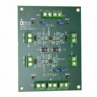
BOARD EVALUATION AD8224
Manufacturer
Analog Devices Inc
Specifications of AD8224-EVALZ
Channels Per Ic
2 - Dual
Amplifier Type
Instrumentation
Output Type
Single-Ended, Rail-to-Rail
Slew Rate
2 V/µs
-3db Bandwidth
1.5MHz
Current - Output / Channel
15mA
Operating Temperature
-40°C ~ 85°C
Current - Supply (main Ic)
750µA
Voltage - Supply, Single/dual (±)
4.5 V ~ 36 V, ±2.25 V ~ 18 V
Board Type
Fully Populated
Utilized Ic / Part
AD8224
Silicon Manufacturer
Analog Devices
Application Sub Type
JFET Input Instrumentation Amplifier
Kit Application Type
Amplifier
Silicon Core Number
AD8224
Kit Contents
Board
Lead Free Status / RoHS Status
Lead free / RoHS Compliant
Available stocks
Company
Part Number
Manufacturer
Quantity
Price
Company:

Part Number:
AD8224-EVALZ
Manufacturer:
Analog Devices Inc
Quantity:
135


Table 12. Gains Achieved Using 1% Resistors
1% Standard Table Value of R
49.9 k
12.4 k
5.49 k
2.61 k
1.00 k
499
249
100
49.9
The AD8224 defaults to G = 1 when no gain resistor is used.
The tolerance and gain drift of the R
to the AD8224 specifications to determine the total gain
accuracy of the system. When the gain resistor is not used,
gain error and gain drift are kept to a minimum.
REFERENCE TERMINAL
The output voltage of the AD8224 is developed with respect to
the potential on the reference terminal. This is useful when the
output signal needs to be offset to a precise midsupply level. For
example, a voltage source can be tied to the REF1 pin or the
REF2 pin to level-shift the output so that the AD8224 can drive
a single-supply ADC. Pin REFx is protected with ESD diodes
and should not exceed either +V
For best performance, source impedance to the REF terminal
should be kept below 1 Ω. As shown in Figure 55, the reference
terminal, REF, is at one end of a 20 kΩ resistor. Additional
impedance at the REF terminal adds to this 20 kΩ resistor and
results in amplification of the signal connected to the positive
input. The amplification from the additional R
computed by
Only the positive signal path is amplified; the negative path is
unaffected. This uneven amplification degrades the CMRR of
the amplifier.
V
REF
INCORRECT
AD8224
2
40
(
20
kΩ
kΩ
+
+
R
R
REF
Figure 56. Driving the Reference Pin
REF
V
REF
)
+
OP2177
–
CORRECT
AD8224
G
(Ω)
S
or −V
G
resistor should be added
S
by more than 0.5 V.
V
Calculated Gain
1.990
4.984
9.998
19.93
50.40
100.0
199.4
495.0
991.0
REF
REF
+
AD8224
–
CORRECT
can be
AD8224
Rev. B | Page 21 of 28
LAYOUT
The AD8224 is a high precision device. To ensure optimum
performance at the PCB level, care must be taken in the design
of the board layout. The AD8224 pinout is arranged in
a logical manner to aid in this task.
Package Considerations
The AD8224 is available in two version s of the 16-lead, 4 mm ×
4 mm LFCSP package: with or without an exposed paddle. Blindly
copying the footprint from another 4 mm × 4 mm LFCSP part
is not recommended because it may not have the same thermal
pad size and leads. Refer to the Outline Dimensions section to
verify that the PCB symbol has the correct dimensions.
Hidden Paddle Package
The AD8224 is available in an LFCSP package with a hidden
paddle. It is the preferred package for the AD8224. Unlike
chip scale packages where the pad limits routing capability,
this package allows routes and vias directly underneath the
chip, so that the full space savings of the small LFCSP can be
realized. Although the package has no metal in the center of
the part, the manufacturing process does leave a very small
section of exposed metal at each of the package corners, shown
in Figure 57 as well as Figure 68 in the Outline Dimensions
section. This metal is connected to +V
Because of a possibility of a short, vias should not be placed
underneath these exposed metal tabs.
Exposed Paddle Package
The AD8224 4 mm × 4 mm LFCSP is also available with an
exposed thermal paddle package version. This pad is connected
internally to +V
connected to the positive supply rail. Space between the leads
and thermal pad should be kept as wide as possible for the best
bias current performance. To maintain the AD8224 ultralow
bias current performance, the thermal pad area can be reduced
to extend the gap between the leads and the pad.
To preserve maximum pin compatibility with other dual
instrumentation amplifiers, such as the AD8222, leave the pad
unconnected. This can be done by not soldering the paddle at
all or by soldering the part to a landing that is a not connected
to any other net. For high vibration applications, a landing is
recommended.
NOTES
1. EXPOSED LEAD FRAME TABS AT THE FOUR CORNERS
OF THE PACKAGE ARE INTERNALLY CONNECTED TO
+V
FURTHER INFORMATION ON PACKAGE AVAILABILITY.
Figure 57. Hidden Paddle Package: Bottom View
S
. REFER TO THE OUTLINE DIMENSIONS PAGE, FOR
S
. The pad can either be left unconnected or
BOTTOM VIEW
S
HIDDEN
PADDLE
EXPOSED LEAD
FRAME TABS
through the part.
AD8224
Related parts for AD8224-EVALZ
Image
Part Number
Description
Manufacturer
Datasheet
Request
R

Part Number:
Description:
Single Supply, Rail to Rail Low Power FET-Input Op Amp
Manufacturer:
Analog Devices
Datasheet:

Part Number:
Description:
±1.7g Dual-Axis IMEMS Accelerometer Evaluation Board
Manufacturer:
Analog Devices Inc
Datasheet:

Part Number:
Description:
Inertial Sensor Evaluation System
Manufacturer:
Analog Devices Inc
Datasheet:
Part Number:
Description:
Manufacturer:
Analog Devices Inc
Datasheet:
Part Number:
Description:
Manufacturer:
Analog Devices Inc
Datasheet:
Part Number:
Description:
Manufacturer:
Analog Devices Inc
Datasheet:
Part Number:
Description:
Manufacturer:
Analog Devices Inc
Datasheet:
Part Number:
Description:
Manufacturer:
Analog Devices Inc
Datasheet:
Part Number:
Description:
Manufacturer:
Analog Devices Inc
Datasheet:
Part Number:
Description:
Manufacturer:
Analog Devices Inc
Datasheet:
Part Number:
Description:
Manufacturer:
Analog Devices Inc
Datasheet:
Part Number:
Description:
Manufacturer:
Analog Devices Inc
Datasheet:
Part Number:
Description:
Manufacturer:
Analog Devices Inc
Datasheet: