ADIS16100/PCB Analog Devices Inc, ADIS16100/PCB Datasheet - Page 14
ADIS16100/PCB
Manufacturer Part Number
ADIS16100/PCB
Description
BOARD EVALUATION ADIS16100
Manufacturer
Analog Devices Inc
Series
iSensor™r
Specifications of ADIS16100/PCB
Sensor Type
Gyroscope, 1 Axis
Sensing Range
±300°/sec
Interface
SPI Serial
Voltage - Supply
4.75 V ~ 5.25 V
Embedded
No
Utilized Ic / Part
ADIS16100
Silicon Manufacturer
Analog Devices
Application Sub Type
Angular Rate Sensor / Gyroscope
Kit Application Type
Sensing - Motion / Vibration / Shock
Silicon Core Number
ADIS16100
Kit Contents
Board
Lead Free Status / RoHS Status
Contains lead / RoHS non-compliant
For Use With
ADISUSBZ - KIT EVAL ADIS W/SOFTWARE USBADISEVALZ - KIT PC EVALUATION W/SOFTWARE
Sensitivity
-
Lead Free Status / Rohs Status
Not Compliant


ADIS16100
APPLICATIONS INFORMATION
ASSEMBLY
The ADIS16100 is a system-in-package (SIP) that integrates
multiple components in a land grid array (LGA). This config-
uration offers the convenience of solder-reflow installation on
printed circuit boards (PCBs). When developing a process flow
for installing ADIS16100 devices on PCBs, see JEDEC standard
document, J-STD-020C, for reflow temperature profile and
processing information. The ADIS16100 can use the Sn-PB
eutectic process from this standard. See JEDEC J-STD-033 for
moisture sensitivity (MSL) handling requirements. The MSL
rating for these devices is marked on the antistatic bags, which
protect these devices from ESD during shipping and handling.
Prior to assembly, review the process flow for information
about introducing shock levels that exceed the ADIS16100’s
absolute maximum ratings. Some PCB separation and
ultrasonic cleaning processes are common areas that can
introduce high levels of shock to these devices.
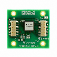
INTERFACE BOARD
The ADIS16100/PCBZ (see the Ordering Guide) provides the
ADIS16100 functionality on a 1.2 inch × 1.3 inch printed circuit
board, which simplifies the connection to an existing processor
system. The four mounting holes accommodate either M2 (2 mm)
or 2-56 machine screws. These boards are made of IS410 material
and are 0.063 inches thick. The second level assembly uses a
SnPb63/37-compatible solder composition, which has a presolder
reflow thickness of approximately 0.005 inches. The pad pattern
on the ADIS16100/PCBZ matches Figure 5. J1 and J2 are dual-
row, 2 mm (pitch) connectors that work with several ribbon
cable systems, including 3M Part Number 152212-0100-GB
(ribbon-crimp connector) and 3M Part Number 3625/12
(ribbon cable).
Rev. D | Page 14 of 16
2 × 0.925
2 × 0.673
2 × 0.000
1.050
0.150
J1
C1
1µF
11
1
3
5
7
9
Figure 24. PCB Assembly View and Dimensions
10
12
2
4
6
8
J1
Figure 23. Electrical Schematic
C1
C4
1µF
12
16
13
14
2
3
1
7
a
ADIS16100
ST2
SCLK
CS
DOUT
ST1
DIN
V
V
CC
DRIVE
i Sensor
U1
RATE
V
GND
FILT
AIN1
AIN2
REF
NC
NC
6
5
4
15
10
11
8
9
C3
1µF
J2
C2
1µF
11
1
3
5
7
9
10
12
2
4
6
8
4 × Ø0.087
M2×0.4
J2
Related parts for ADIS16100/PCB
Image
Part Number
Description
Manufacturer
Datasheet
Request
R

Part Number:
Description:
±1.7g Dual-Axis IMEMS Accelerometer Evaluation Board
Manufacturer:
Analog Devices Inc
Datasheet:

Part Number:
Description:
Inertial Sensor Evaluation System
Manufacturer:
Analog Devices Inc
Datasheet:
Part Number:
Description:
Manufacturer:
Analog Devices Inc
Datasheet:
Part Number:
Description:
Manufacturer:
Analog Devices Inc
Datasheet:
Part Number:
Description:
Manufacturer:
Analog Devices Inc
Datasheet:
Part Number:
Description:
Manufacturer:
Analog Devices Inc
Datasheet:
Part Number:
Description:
Manufacturer:
Analog Devices Inc
Datasheet:
Part Number:
Description:
Manufacturer:
Analog Devices Inc
Datasheet:
Part Number:
Description:
Manufacturer:
Analog Devices Inc
Datasheet:
Part Number:
Description:
Manufacturer:
Analog Devices Inc
Datasheet:
Part Number:
Description:
Manufacturer:
Analog Devices Inc
Datasheet:
Part Number:
Description:
Manufacturer:
Analog Devices Inc
Datasheet:
Part Number:
Description:
Manufacturer:
Analog Devices Inc
Datasheet: