CYII4SC6600-EVAL Cypress Semiconductor Corp, CYII4SC6600-EVAL Datasheet - Page 10
CYII4SC6600-EVAL
Manufacturer Part Number
CYII4SC6600-EVAL
Description
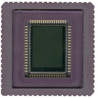
BOARD EVAL IMAGE SENS IBIS4-6600
Manufacturer
Cypress Semiconductor Corp
Datasheet
1.CYII4SC6600-EVAL.pdf
(34 pages)
Specifications of CYII4SC6600-EVAL
Sensor Type
CMOS Imaging, Color (RGB)
Sensing Range
6.6 Megapixel
Interface
SPI
Sensitivity
89 fps
Voltage - Supply
2.5 V ~ 3.3 V
Embedded
No
Utilized Ic / Part
IBIS4-6600
Lead Free Status / RoHS Status
Contains lead / RoHS non-compliant
Lead Free Status / RoHS Status
Lead free / RoHS Compliant, Contains lead / RoHS non-compliant


Stage 1: Offset, FPN Correction, and Multiplexing
In the first stage, the signals from the buses are subtracted and
the offset from the DACs is added. After a system reset, the
analog multiplexer is configured for two outputs (see the bit
settings in the
ONE_OUT is set to 1, the two signals S1 and S2 are multiplexed
to one output (output 1). The amplifiers of Stage 2 and Stage 3
of the second output path are then put in standby. The speed and
power consumption of the first stage can be controlled through
the resistor connected to CMD_OUT_1.
Stage 2: Programmable Gain Amplifier
The second stage provides the gain, which is adjustable
between 1.36 and 17.38 in steps of approximately 20.25 (~1.2).
An overview of the gain settings is given in
and power consumption of the second stage can be controlled
through the resistor connected to CMD_OUT_2.
Table 4. PGA Gain Settings
Document Number: 001-02366 Rev. *G
0000
0001
0010
0011
0100
0101
0110
0111
Bits
AMPLIFIER Register
DC Gain
+
1.36
1.64
1.95
2.35
2.82
3.32
3.93
4.63
VCAL
RCAL
D
D
AC
AC
Figure 11. Offset for the Two Channels through DAC_RAW and DAC_FINE
_
_
RAW
FINE
_
_
pad
REG
REG
floating
1000
1001
1010
1011
1100
1101
1110
1111
Bits
<0:7
<0:7
RCAL
on page 22). In case
_
DAC
Table
DAC_raw
DAC_fine
_
OUT
rcal
rcal
DC Gain
4. The speed
10.31
12.36
14.67
17.38
5.40
6.35
7.44
8.79
out
out
VDDA
GNDA
50K
50K
Stage 3: Output Drivers
The speed and power consumption of the third stage can be
controlled through the resistor connected to CMD_OUT_3. The
output drivers are designed to drive a 20 pF output load at
40 Msamples/s with a bias resistor of 100 k.
Offset DACs
Figure 11
reference voltages of the two different channels. The offset is
mainly given through DAC_raw. DAC_fine can be used to shift
the reference voltage of bus 2 up or down to compensate for
different offsets in the two channels.
Note that in this figure, “K” represents K
shows how the DAC registers influence the black
IBIS4-6600 CYII4SM6600AB
10K
10K
200K
200K
blackref
blackref
bus1
bus2
Page 10 of 34
[+] Feedback
Related parts for CYII4SC6600-EVAL
Image
Part Number
Description
Manufacturer
Datasheet
Request
R

Part Number:
Description:
Manufacturer:
Cypress Semiconductor Corp
Datasheet:
Part Number:
Description:
Manufacturer:
Cypress Semiconductor Corp
Datasheet:
Part Number:
Description:
Manufacturer:
Cypress Semiconductor Corp
Datasheet:
Part Number:
Description:
Manufacturer:
Cypress Semiconductor Corp
Datasheet:
Part Number:
Description:
Manufacturer:
Cypress Semiconductor Corp
Datasheet: