CYII4SC6600-EVAL Cypress Semiconductor Corp, CYII4SC6600-EVAL Datasheet - Page 9
CYII4SC6600-EVAL
Manufacturer Part Number
CYII4SC6600-EVAL
Description
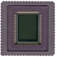
BOARD EVAL IMAGE SENS IBIS4-6600
Manufacturer
Cypress Semiconductor Corp
Datasheet
1.CYII4SC6600-EVAL.pdf
(34 pages)
Specifications of CYII4SC6600-EVAL
Sensor Type
CMOS Imaging, Color (RGB)
Sensing Range
6.6 Megapixel
Interface
SPI
Sensitivity
89 fps
Voltage - Supply
2.5 V ~ 3.3 V
Embedded
No
Utilized Ic / Part
IBIS4-6600
Lead Free Status / RoHS Status
Contains lead / RoHS non-compliant
Lead Free Status / RoHS Status
Lead free / RoHS Compliant, Contains lead / RoHS non-compliant


Pixel Rate
The pixel rate for this sensor is high enough to support a frame
rate greater than 75 Hz for a window size of 640 x 480 pixels
(VGA format), and 23 pixels over scan in both directions. Taking
into account a row blanking time of 7.2 µs (as baseline, refer the
following calculations), this requires a minimum pixel rate of
approximately 40 MHz. The final bandwidth of the column
amplifiers, output stage, and more is determined by external bias
resistors. Taking into account a pixel rate of 40 MHz, a full frame
rate of a little more than 5 frames/s is obtained.
The frame period of the IBIS4-6600 sensor is calculated as:
In this equation:
Nr. Lines: Number of Lines read out each frame (Y)
Nr. Pixels: Number of pixels read out each line (X)
RBT: Row Blanking Time = 7.2 µs (typical)
Table 3. Frame Rate vs. Resolution
Output Amplifier
The output amplifier subtracts the reset and signal voltages from
each other to cancel FPN as much as possible (shown in
Figure
of two DACs. One DAC is used for the main offset (DAC_raw).
The other enables fine tuning to compensate the offset difference
between the signal paths arriving at the two amplifiers A1 and A2
(DAC_fine). With the analog multiplexer, the signals S1 and S2
from the two buses can be combined to one pixel output at full
pixel rate (40 MHz). However, the two analog signals S1 and S2
can also be available on two separate output pins to allow a
higher pixel rate.
Document Number: 001-02366 Rev. *G
=> Frame period = (Nr. Lines * (RBT + pixel period * Nr. Pixels))
3002 x 2210
1501 x 1104
640 x 480
Image Resolution (Y*X)
10). The DAC that is used for offset adjustment consists
bus1 S
bus1_R
bus2 S
bus2_R
Frame Rate [frames/s]
DAC_raw /
DAC_dark
DAC_fine
+
+
A2
A1
Figure 10. Output Amplifier Architecture
14
89
5
S2
S1
multiplexer
Stage 1
analog
Frame Readout Time [ms]
Pixel period: 1/40 MHz = 25 ns
Example: Read out time of the full resolution at nominal speed
(40 MHz pixel rate):
=> 5.33 fps.
Region of Interest (ROI) Read Out
Windowing is easily achieved by uploading the starting point of
the x and y-shift registers in the sensor registers (refer
on page 17). This downloaded starting point initiates the shift
register in the x and y-direction, triggered by the Y_START
(initiates the Y-shift register) and the Y_CLK (initiates the X-shift
register) pulse. The minimum step size for the x-address is 24
(only even start addresses can be chosen) and 1 for the
Y-address (every line can be addressed). The frame rate
increases in an almost linear manner when fewer pixels are read
out.
The third DAC (DAC_dark) puts its value on the buses during the
calibration of the output amplifier. In case of nondestructive
readout (no double sampling), bus1_R and bus2_R are
continuously connected to the output of the DAC_fine to provide
a reference for the signals on bus1_S and bus2_S.
The complete output amplifier can be put in standby by setting
the corresponding bit in the AMPLIFIER register.
=> Frame period = (3002 * (7.2 µs + 25 ns * 2210)) = 187.5 ms
programmable
gain amplifiers
Table 3
187.5
Stage 2
67
11
lists the achievable frame rates with ROI read out.
IBIS4-6600 CYII4SM6600AB
drivers
output
Full resolution
ROI read out
11
Stage 3
1
1
Pixel output 2
Pixel output
Comment
Page 9 of 34
Table 10
[+] Feedback
Related parts for CYII4SC6600-EVAL
Image
Part Number
Description
Manufacturer
Datasheet
Request
R

Part Number:
Description:
Manufacturer:
Cypress Semiconductor Corp
Datasheet:
Part Number:
Description:
Manufacturer:
Cypress Semiconductor Corp
Datasheet:
Part Number:
Description:
Manufacturer:
Cypress Semiconductor Corp
Datasheet:
Part Number:
Description:
Manufacturer:
Cypress Semiconductor Corp
Datasheet:
Part Number:
Description:
Manufacturer:
Cypress Semiconductor Corp
Datasheet: