CYII4SC6600-EVAL Cypress Semiconductor Corp, CYII4SC6600-EVAL Datasheet - Page 28
CYII4SC6600-EVAL
Manufacturer Part Number
CYII4SC6600-EVAL
Description
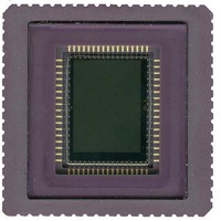
BOARD EVAL IMAGE SENS IBIS4-6600
Manufacturer
Cypress Semiconductor Corp
Datasheet
1.CYII4SC6600-EVAL.pdf
(34 pages)
Specifications of CYII4SC6600-EVAL
Sensor Type
CMOS Imaging, Color (RGB)
Sensing Range
6.6 Megapixel
Interface
SPI
Sensitivity
89 fps
Voltage - Supply
2.5 V ~ 3.3 V
Embedded
No
Utilized Ic / Part
IBIS4-6600
Lead Free Status / RoHS Status
Contains lead / RoHS non-compliant
Lead Free Status / RoHS Status
Lead free / RoHS Compliant, Contains lead / RoHS non-compliant


Table 15. Pin List (continued)
Document Number: 001-02366 Rev. *G
29
30
31
32
33
34
35
36
37
38
39
40
41
42
43
44
45
46
47
48
49
50
51
52
53
54
55
56
57
58
59
60
61
62
63
Pin
V
REG_CLOCK
SYS_CLOCK
SYS_RESET
Y_CLK
Y_START
GNDD_ADC
VDDD_ADC
GNDA_ADC
VDDA_ADC
VHIGH_ADC
VLOW_ADC
GNDA_ADC
VDDA_ADC
GNDD_ADC
VDDD_ADC
VDD_RESET_DS
ADC_CLK_EXT
EOL
EOF
PIX_VALID
TEMP
ADC_D<9>
VDD_PIX
GND_AB
ADC_D<8>
ADC_D<7>
ADC_D<6>
ADC_D<5>
ADC_D<4>
ADC_D<3>
VDD_RESET
ADC_D<2>
ADC_D<1>
ADC_D<0>
DDA
Pin Name
Pin Type
Output
Output
Output
Output
Output
Output
Output
Output
Output
Output
Output
Output
Output
Output
Power
Power
Power
Power
Power
Power
Power
Power
Power
Power
Power
Power
Power
Input
Input
Input
Input
Input
Input
Input
Input
2.5
-
-
-
-
-
0
2.5
0
2.5
1.5
0.42
0
2.5
0
2.5
2.5 (for no dual slope)
-
-
-
-
-
-
2.5
0
-
-
-
-
-
-
2.5
-
-
-
Expected Voltage [V]
V
Register clock. Data on internal bus is copied to
corresponding registers on rising edge.
System clock defining the pixel rate (nominal 40 MHz, 50% ±
5% duty cycle)
Global system reset (active high)
Line clock
Start frame readout
GND (&substrate) of digital part ADC
V
GND (&substrate) of analog part
V
ADC high reference voltage (for example, connect to
VDDA_ADC with R = 560 and decouple to GNDA_ADC with
C = 100 nF)
ADC low reference voltage (for example, connect to
GNDA_ADC with R = 220 and decouple to GNDA_ADC
with C = 100 nF)
GND (&substrate) of analog part
V
GND (&substrate) of digital part ADC
V
Variable reset voltage (dual slope)
External ADC clock
Diagnostic end of line signal (produced by sequencer), can
be used as Y_CLK
Diagnostic end of frame signal (produced by sequencer), can
be used as Y_START
Diagnostic signal. High during pixel readout
Temperature measurement. Output voltage varies linearly
with temperature.
ADC data output (MSB)
V
Anti-blooming ground. Set to 1V for improved anti-blooming
behavior
ADC data output
ADC data output
ADC data output
ADC data output
ADC data output
ADC data output
Reset voltage [2.5V]. Highest voltage to the chip. 3.3V for
extended dynamic range or 'hard reset'.
ADC data output
ADC data output
ADC data output (LSB)
DD
DD
DD
DD
DD
DD
of analog part [2.5V]
of digital part [2.5V] ADC
of analog part [2.5V]
of analog part [2.5V]
of digital part [2.5V] ADC
of pixel core [2.5V]
IBIS4-6600 CYII4SM6600AB
Pin Description
Page 28 of 34
[+] Feedback
Related parts for CYII4SC6600-EVAL
Image
Part Number
Description
Manufacturer
Datasheet
Request
R

Part Number:
Description:
Manufacturer:
Cypress Semiconductor Corp
Datasheet:
Part Number:
Description:
Manufacturer:
Cypress Semiconductor Corp
Datasheet:
Part Number:
Description:
Manufacturer:
Cypress Semiconductor Corp
Datasheet:
Part Number:
Description:
Manufacturer:
Cypress Semiconductor Corp
Datasheet:
Part Number:
Description:
Manufacturer:
Cypress Semiconductor Corp
Datasheet: