DM164120-1 Microchip Technology, DM164120-1 Datasheet - Page 25
DM164120-1
Manufacturer Part Number
DM164120-1
Description
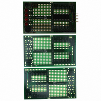
BOARD DEMO PICKIT 2 LP COUNT
Manufacturer
Microchip Technology
Type
MCUr
Datasheet
1.DM164120-1.pdf
(42 pages)
Specifications of DM164120-1
Contents
3 Boards (1 Populated, 2 Bare)
Processor To Be Evaluated
PIC16F690
Silicon Manufacturer
Microchip
Core Architecture
PIC
Core Sub-architecture
PIC16
Silicon Core Number
PIC16F
Silicon Family Name
PIC16F6xxx
Rohs Compliant
Yes
Lead Free Status / RoHS Status
Lead free / RoHS Compliant
For Use With/related Products
28-pin PIC16C, 16F, 18C, 18F
Lead Free Status / Rohs Status
Lead free / RoHS Compliant
Available stocks
Company
Part Number
Manufacturer
Quantity
Price
Company:

Part Number:
DM164120-1
Manufacturer:
Microchip Technology
Quantity:
135


© 2005 Microchip Technology Inc.
bit 7
bit 6
bit 5-2
bit 1
bit 0
3.2.4.2
ADCON0 controls the ADC operation. Bit 0 turns on the ADC module. Bit 1 starts a
conversion and bits <5:2> selects which channel the ADC will operate. VCFG bit< 6>
selects the ADC reference, which may be either V
on V
For purposes of this lesson, the ADC must be turned on and pointed to RA0. Choose
the internal voltage reference and 8T
The ADC needs about 5 μs, after changing channels, to allow the ADC sampling
capacitor to settle. Finally, we can start the conversion by setting the GO bit in ADCON0.
The bit also serves as the DONE flag. That is, the ADC will clear the same bit when the
conversion is complete. The answer is then available in ADRESH:ADRESL.
This lesson takes the high order 4 bits of the result and copies them to the display LEDs
attached to PORTC.
See the Analog-to-Digital section in the PIC16F685/687/689/690 Data Sheet
(DS41262) for more details on the ADC module.
REGISTER 3-2:
bit 7
ADFM: A/D Result Formed Select bit
1 = Right justified
0 = Left justified
VCFG: Voltage Reference bit
1 = V
0 = V
CHS<3:0>: Analog Channel Select bits
0000 = Channel 00 (AN0)
0001 = Channel 01 (AN1)
0010 = Channel 02 (AN2)
0011 = Channel 03 (AN3)
0100 = Channel 04 (AN4)
0101 = Channel 05 (AN5)
0110 = Channel 06 (AN6)
0111 = Channel 07 (AN7)
1000 = Channel 08 (AN8)
1001 = Channel 09 (AN9)
1010 = Channel 10 (AN10)
1011 = Channel 11 (AN11)
1100 = CV
1101 = VP6
1110 = Reserved. Do not use.
1111 = Reserved. Do not use.
GO/DONE: A/D Conversion Status bit
1 = A/D conversion cycle in progress. Setting this bit starts an A/D conversion cycle.
0 = A/D conversion completed/not in progress
ADON: A/D Enable bit
1 = A/D converter module is enabled
0 = A/D converter is shut off and consumes no operating current
Legend:
R = Readable bit
- n = Value at POR
R/W-0
ADFM
This bit is automatically cleared by hardware when the A/D conversion has completed.
REF
REF
DD
. ADFM bit <7> selects whether the 10 bits are right or left justified in the 16 bits.
pin
ADCON0
REF
R/W-0
VCFG
ADCON0 – A/D CONTROL REGISTER (ADDRESS: 1Fh)
R/W-0
CHS3
W = Writable bit
‘1’ = Bit is set
R/W-0
LPC Demo Board Lessons
CHS2
OSC
conversion clock.
R/W-0
CHS1
U = Unimplemented bit, read as ‘0’
‘0’ = Bit is cleared
DD
or a separate reference voltage
R/W-0
CHS0
GO/DONE
x = Bit is unknown
R/W-0
DS51556A-page 21
R/W-0
ADON
bit 0
Related parts for DM164120-1
Image
Part Number
Description
Manufacturer
Datasheet
Request
R

Part Number:
Description:
SERIES CONNECTION; 16 DIODES
Manufacturer:
Altech Corp.
Datasheet:

Part Number:
Description:
Manufacturer:
Microchip Technology Inc.
Datasheet:
Part Number:
Description:
Manufacturer:
Microchip Technology Inc.
Datasheet:
Part Number:
Description:
Manufacturer:
Microchip Technology Inc.
Datasheet:
Part Number:
Description:
Manufacturer:
Microchip Technology Inc.
Datasheet:
Part Number:
Description:
Manufacturer:
Microchip Technology Inc.
Datasheet:
Part Number:
Description:
Manufacturer:
Microchip Technology Inc.
Datasheet:
Part Number:
Description:
Manufacturer:
Microchip Technology Inc.
Datasheet:
Part Number:
Description:
Manufacturer:
Microchip Technology Inc.
Datasheet: