DV164101 Microchip Technology, DV164101 Datasheet - Page 31
DV164101
Manufacturer Part Number
DV164101
Description
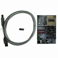
KIT DEV PICKIT1 FLASH 8/14PIN
Manufacturer
Microchip Technology
Series
PICkit™ 1r
Type
MCUr
Specifications of DV164101
Contents
PIC Kit 1 Circuit Board, CD-ROMs, USB Interface Cable and Booklet
Processor To Be Evaluated
PIC12F675
Interface Type
USB
Silicon Manufacturer
Microchip
Core Architecture
PIC
Core Sub-architecture
PIC12, PIC16
Silicon Core Number
PIC12F, PIC16F
Silicon Family Name
PIC12F6xx, PIC16F6xx
Rohs Compliant
NA
Lead Free Status / RoHS Status
Lead free / RoHS Compliant
For Use With/related Products
Microchip's 8-14 Pin FLASH Microcontrollers
For Use With
AC164122 - BOARD DAUGHT PICTAIL SD/MMC CARDAC164120 - BOARD SIGNAL ANALYSIS PICKIT
Lead Free Status / Rohs Status
Lead free / RoHS Compliant
Other names
DV164101R
DV164101R
DV164101R
Available stocks
Company
Part Number
Manufacturer
Quantity
Price
Company:

Part Number:
DV164101
Manufacturer:
Microchip Technology
Quantity:
135


A.1
A.2
A.3
A.4
2004 Microchip Technology Inc.
INTRODUCTION
HIGHLIGHTS
IN-CIRCUIT SERIAL PROGRAMMING™ (ICSP™)
PROGRAMMING HARDWARE
This appendix contains the PICkit™ 1 hardware description and schematic diagrams.
This appendix discusses:
• In-Circuit Serial Programming™ (ICSP™)
• Programming Hardware
• USB Communications Protocol
• Schematic Diagrams:
In-Circuit Serial Programming (ICSP) allows an engineer to design a circuit that will be
built and then programmed later. ICSP is described in the programming specifications
documentation. These documents can be found on the Microchip web site
(http:\\www.microchip.com). ICSP requires a 12-13V power supply, control of the V
supply and two I/O pins to clock in commands and data.
The programmer portion of the PICkit 1 Flash Starter Kit circuit is shown in Figure A-1.
Additional circuitry is present to connect to the USB and drive the evaluation LEDs.
Most of the circuitry in the figure is used to generate the +13V required for V
generated by using the CCP of the PIC16C745 to pulse Q2 on and off. By pulsing Q2,
L1 generates a burst of charge that is steered into the capacitor C4 by the diode D13.
Each burst of charge adds to the voltage already in the capacitor. The size of the burst
of charge is proportional to the on time of the PWM signal from CCP. The resistors R10
and R11 form a voltage divider that drops the 13V V
is measured by AN1. Software running in the PIC16C745 periodically samples AN1
and computes a new PWM value. The PWM value is updated just over 500 times every
second. This ensures good voltage regulation of the 13V and leaves enough CPU time
to perform the programming task. The rest of the circuit is used to switch the V
voltage to the V
driver for Q4. Transistor Q1 turns V
The programming I/O signals are generated by software routines on I/O port pins RC6
and RC7 of the PIC16C745, which drive I/O port pins RA0/GP0 (ICSPDAT) and
RA1/GP1 (ICSPCLK) of the target 8 or 14-pin Flash device.
Appendix A. Hardware Description
- PICkit 1 Board Diagram
- LED Layout
- V
- USB Control
- Prototype 1
- Prototype 2
PP
Supply
PP
pin. Transistor Q4 is the switch for the V
PICKIT
DD
™
on and off allowing the target device to be reset.
1 FLASH STARTER KIT
PP
to a 4.5V feedback signal that
USER’S GUIDE
PP
voltage and Q3 is the
DS40051D-page 27
PP
. This is
PP
DD
Related parts for DV164101
Image
Part Number
Description
Manufacturer
Datasheet
Request
R

Part Number:
Description:
Manufacturer:
Microchip Technology Inc.
Datasheet:
Part Number:
Description:
Manufacturer:
Microchip Technology Inc.
Datasheet:
Part Number:
Description:
Manufacturer:
Microchip Technology Inc.
Datasheet:
Part Number:
Description:
Manufacturer:
Microchip Technology Inc.
Datasheet:
Part Number:
Description:
Manufacturer:
Microchip Technology Inc.
Datasheet:
Part Number:
Description:
Manufacturer:
Microchip Technology Inc.
Datasheet:
Part Number:
Description:
Manufacturer:
Microchip Technology Inc.
Datasheet:
Part Number:
Description:
Manufacturer:
Microchip Technology Inc.
Datasheet: