DV164101 Microchip Technology, DV164101 Datasheet - Page 33
DV164101
Manufacturer Part Number
DV164101
Description
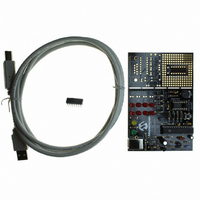
KIT DEV PICKIT1 FLASH 8/14PIN
Manufacturer
Microchip Technology
Series
PICkit™ 1r
Type
MCUr
Specifications of DV164101
Contents
PIC Kit 1 Circuit Board, CD-ROMs, USB Interface Cable and Booklet
Processor To Be Evaluated
PIC12F675
Interface Type
USB
Silicon Manufacturer
Microchip
Core Architecture
PIC
Core Sub-architecture
PIC12, PIC16
Silicon Core Number
PIC12F, PIC16F
Silicon Family Name
PIC12F6xx, PIC16F6xx
Rohs Compliant
NA
Lead Free Status / RoHS Status
Lead free / RoHS Compliant
For Use With/related Products
Microchip's 8-14 Pin FLASH Microcontrollers
For Use With
AC164122 - BOARD DAUGHT PICTAIL SD/MMC CARDAC164120 - BOARD SIGNAL ANALYSIS PICKIT
Lead Free Status / Rohs Status
Lead free / RoHS Compliant
Other names
DV164101R
DV164101R
DV164101R
Available stocks
Company
Part Number
Manufacturer
Quantity
Price
Company:

Part Number:
DV164101
Manufacturer:
Microchip Technology
Quantity:
135


A.5
2004 Microchip Technology Inc.
USB COMMUNICATIONS PROTOCOL
The USB protocol used by the PICkit 1 Flash Starter Kit is a very simple
command/response type protocol. Multiple commands can be put together to fill the 8
bytes of a USB packet. If a command cannot fill the 8 bytes and it is not desired to use
a second command to fill the packet, the packet should be padded with ‘Z’ to indicate
no operation.
A.5.1
• ‘C’ <word> – Configuration Memory Write mode. Word parameter ignored. Use
• ‘c’ – Download Command Table. 15 bytes to follow (two 8 byte packets) containing
• ‘D’ <byte> – Write EE Data memory. Data is passed as the byte.
• ‘E’ – Bulk Erase Program memory
• ‘e’ – Bulk Erase Data memory
• ‘g’ – Get n bytes from device (n is a word)
• ‘I’ <word> – Increment Address N times. N is passed as word.
• ‘P’ – Enter Programming mode. Turns V
• ‘p’ – Exit Programming mode. Turns V
• ‘R’ – Read Program memory. ‘R’ always returns 4 words. If the end of PGM
• ‘r’ – Read EE Data memory. ‘r’ always returns 8 bytes. If the end of Data memory
• ‘S’ <program memory length, data memory length> – Calculates Program
• ‘t’ – Transmit n bytes to device (n is a word)
• ‘V’ <byte> – Power and special feature control. The byte following command is
• ‘v’ – Return version information. The following bytes are returned:
• ‘W’ <word> – Write Program Memory. Loads the write latch, sends the write
The last 4 commands are undefined but the second data packet will be filled out.
‘W’ to write to configuration memory.
the 6-bit commands in the following order:
- Load Configuration memory
- Load data for Program memory
- Load data for EE Data memory
- Read data from Program memory
- Increment Address
- Begin programming (internally timed)
- Begin programming (externally timed)
- End programming (externally timed)
- Bulk Erase Program memory
- Bulk Erase EE Data memory
memory is reached, it pads with 0’s. It is the responsibility of the host software to
determine if padding occurred by keeping track of the program counter.
is reached, it pads with 0’s. It is the responsibility of the host software to determine
if padding occurred by keeping track of the program counter.
Memory Checksum and Data Memory Checksum. The checksum is calculated on
the first N
memory. N
value is 3 bytes in length: the first word is the Program Memory Checksum, and
the last byte is the Data Memory Checksum.
used to control. V
square wave.
<Major><Minor><Dot>.
command and increments to the next address.
Commands
p
p
words of the program memory and the first N
and N
DD
d
are both words passed as the length parameter. The return
power to the target and to enable/disable a 2.5 kHz 50%
DD
PP
and V
and V
PP
DD
off.
on.
d
bytes of the data
DS40051D-page 29
Related parts for DV164101
Image
Part Number
Description
Manufacturer
Datasheet
Request
R

Part Number:
Description:
Manufacturer:
Microchip Technology Inc.
Datasheet:
Part Number:
Description:
Manufacturer:
Microchip Technology Inc.
Datasheet:
Part Number:
Description:
Manufacturer:
Microchip Technology Inc.
Datasheet:
Part Number:
Description:
Manufacturer:
Microchip Technology Inc.
Datasheet:
Part Number:
Description:
Manufacturer:
Microchip Technology Inc.
Datasheet:
Part Number:
Description:
Manufacturer:
Microchip Technology Inc.
Datasheet:
Part Number:
Description:
Manufacturer:
Microchip Technology Inc.
Datasheet:
Part Number:
Description:
Manufacturer:
Microchip Technology Inc.
Datasheet: