QSK-62P PLUS BNS Solutions, QSK-62P PLUS Datasheet - Page 32
QSK-62P PLUS
Manufacturer Part Number
QSK-62P PLUS
Description
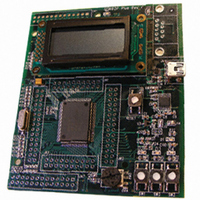
KIT QUICK START RENESAS 62P
Manufacturer
BNS Solutions
Series
M16C™r
Type
MCUr
Datasheet
1.QSK-62P_PLUS.pdf
(103 pages)
Specifications of QSK-62P PLUS
Contents
Board, Cable, CD
For Use With/related Products
M16C/62P
Lead Free Status / RoHS Status
Not applicable / Not applicable
Other names
867-1000
QSK-62P
QSK26A
QSK62P
QSK-62P
QSK26A
QSK62P


M16C/62P Group (M16C/62P, M16C/62PT)
Rev.2.41
REJ03B0001-0241
2.
Figure 2.1 shows the CPU registers. The CPU has 13 registers. Of these, R0, R1, R2, R3, A0, A1 and FB comprise a
register bank. There are two register banks.
Figure 2.1
2.1
The R0 register consists of 16 bits, and is used mainly for transfers and arithmetic/logic operations. R1 to R3 are
the same as R0.
The R0 register can be separated between high (R0H) and low (R0L) for use as two 8-bit data registers.
R1H and R1L are the same as R0H and R0L. Conversely, R2 and R0 can be combined for use as a 32-bit data
register (R2R0). R3R1 is the same as R2R0.
Central Processing Unit (CPU)
Data Registers (R0, R1, R2 and R3)
b31
Jan 10, 2006
Central Processing Unit Register
NOTES:
1. These registers comprise a register bank. There are two register banks.
R2
R3
Page 30 of 96
b15
IPL
b19
b19
INTBH
b15
b15
b15
b15
R0H
R1H
b8
b7
U
PC
I
INTBL
b8 b7
USP
FLG
ISP
SB
R2
R3
A0
A1
FB
O
B
S
R0L
R1L
Z
D
C
b0
b0
b0
b0
b0
b0
2. Central Processing Unit (CPU)
Data Registers
Address Registers
Frame Base Registers
Interrupt Table Register
Program Counter
User Stack Pointer
Interrupt Stack Pointer
Static Base Register
Flag Register
Carry Flag
Debug Flag
Zero Flag
Sign Flag
Register Bank Select Flag
Overflow Flag
Interrupt Enable Flag
Stack Pointer Select Flag
Reserved Area
Processor Interrupt Priority Level
Reserved Area
(1)
(1)
(1)