QSK-62P PLUS BNS Solutions, QSK-62P PLUS Datasheet - Page 55
QSK-62P PLUS
Manufacturer Part Number
QSK-62P PLUS
Description
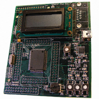
KIT QUICK START RENESAS 62P
Manufacturer
BNS Solutions
Series
M16C™r
Type
MCUr
Datasheet
1.QSK-62P_PLUS.pdf
(103 pages)
Specifications of QSK-62P PLUS
Contents
Board, Cable, CD
For Use With/related Products
M16C/62P
Lead Free Status / RoHS Status
Not applicable / Not applicable
Other names
867-1000
QSK-62P
QSK26A
QSK62P
QSK-62P
QSK26A
QSK62P


M16C/62P Group (M16C/62P, M16C/62PT)
Rev.2.41
REJ03B0001-0241
Switching Characteristics
(V
Figure 5.2
CC1
Table 5.27
NOTES:
t
t
t
t
t
t
t
t
t
t
t
t
t
t
t
th(WR-DB)
t
d(BCLK-AD)
h(BCLK-AD)
h(RD-AD)
h(WR-AD)
d(BCLK-CS)
h(BCLK-CS)
d(BCLK-ALE)
h(BCLK-ALE)
d(BCLK-RD)
h(BCLK-RD)
d(BCLK-WR)
h(BCLK-WR)
d(BCLK-DB)
h(BCLK-DB)
d(DB-WR)
d(BCLK-HLDA)
Symbol
1. Calculated according to the BCLK frequency as follows:
2. Calculated according to the BCLK frequency as follows:
3. This standard value shows the timing when the output is off, and
= V
does not show hold time of data bus.
Hold time of data bus varies with capacitor volume and pull-up
(pull-down) resistance value.
Hold time of data bus is expressed in
by a circuit of the right figure.
For example, when V
of output ”L” level is
CC2
Jan 10, 2006
----------------------- - 40 ns
f BCLK
----------------------- - 10 ns
f BCLK
0.5x10
0.5x10
t = − CR X ln (1 − V
t = − 30pF X 1k Ω X In(1 − 0.2V
(
(
= 6.7ns.
= 5V, V
Address Output Delay Time
Address Output Hold Time (in relation to BCLK)
Address Output Hold Time (in relation to RD)
Address Output Hold Time (in relation to WR)
Chip Select Output Delay Time
Chip Select Output Hold Time (in relation to BCLK)
ALE Signal Output Delay Time
ALE Signal Output Hold Time
RD Signal Output Delay Time
RD Signal Output Hold Time
WR Signal Output Delay Time
WR Signal Output Hold Time
Data Output Delay Time (in relation to BCLK)
Data Output Hold Time (in relation to BCLK)
Data Output Delay Time (in relation to WR)
Data Output Hold Time (in relation to WR)
HLDA Output Delay Time
9
9
Ports P0 to P14 Measurement Circuit
Memory Expansion and Microprocessor Modes (for setting with no wait)
)
)
–
–
SS
[
[
= 0V, at T
]
]
OL
OL
Page 53 of 96
/ V
= 0.2V
CC2
)
f(BCLK) is 12.5MHz or less.
CC2
opr
CC2
, C = 30pF, R = 1k Ω , hold time
Parameter
= −20 to 85°C / −40 to 85°C unless otherwise specified)
/ V
CC2
)
P0
P1
P2
P3
P4
P5
P6
P7
P8
P9
P10
P11
P12
P13
P14
(3)
(3)
30pF
See
Figure 5.2
(NOTE 2)
(NOTE 1)
(NOTE 2)
V
DBi
Min.
CC1
− 4
5. Electrical Characteristics
4
0
4
0
0
4
Standard
=V
Max.
25
25
15
25
25
40
40
CC2
C
R
=5V
Unit
ns
ns
ns
ns
ns
ns
ns
ns
ns
ns
ns
ns
ns
ns
ns
ns
ns