EVAL-ADUC842QS Analog Devices Inc, EVAL-ADUC842QS Datasheet - Page 4
EVAL-ADUC842QS
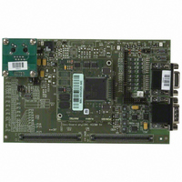
Manufacturer Part Number
EVAL-ADUC842QS
Description
KIT DEV FOR ADUC842 QUICK START
Manufacturer
Analog Devices Inc
Series
QuickStart™ Kitr
Type
MCUr
Datasheet
1.EVAL-ADUC842QS.pdf
(88 pages)
Specifications of EVAL-ADUC842QS
Contents
Evaluation Board, Power Supply, Cable, Software and Documentation
Lead Free Status / RoHS Status
Contains lead / RoHS non-compliant
For Use With/related Products
ADuC842
Lead Free Status / RoHS Status
Not Compliant, Contains lead / RoHS non-compliant


ADuC841/ADuC842/ADuC843
Parameter
DAC AC CHARACTERISTICS
DAC CHANNEL SPECIFICATIONS
Internal Buffer Disabled ADuC841/ADuC842 Only
DC ACCURACY
ANALOG OUTPUTS
REFERENCE INPUT/OUTPUT REFERENCE OUTPUT
EXTERNAL REFERENCE INPUT
POWER SUPPLY MONITOR (PSM)
WATCHDOG TIMER (WDT)
FLASH/EE MEMORY RELIABILITY CHARACTERISTICS
DIGITAL INPUTS
RESET
Voltage Output Settling Time
Digital-to-Analog Glitch Energy
Resolution
Relative Accuracy
Differential Nonlinearity
Offset Error
Gain Error
Gain Error Mismatch
Voltage Range_0
Output Voltage (V
Accuracy
Power Supply Rejection
Reference Temperature Coefficient
Internal V
Voltage Range (V
Input Impedance
Input Leakage
DV
DV
Timeout Period
Endurance
Data Retention
Input Leakage Current (Port 0, EA )
Logic 1 Input Current
(All Digital Inputs), SDATA, SCLOCK
Logic 0 Input Current (Ports 1, 2, 3) SDATA, SCLOCK
Logic 1 to Logic 0 Transition Current (Ports 2 and 3)
DD
DD
Trip Point Selection Range
Power Supply Trip Point Accuracy
REF
17
10
Power-On Time
18
REF
REF
)
)
4
4
4
11
15
12, 13
14
16
V
15
10
12
±3
–1
±1/2
±5
±0.5
0.5
0 to V
2.5
±10
65
±15
2
1
V
20
1
0
2000
100,000
100
±10
±1
±10
±1
–75
–40
–660
–400
±10
10
105
Rev. 0 | Page 4 of 88
DD
DD
= 5 V
REF
V
15
10
12
±3
–1
±1/2
±5
±0.5
0.5
0 to V
2.5
±10
67
±15
2
1
V
20
1
2.93
3.08
±2.5
0
2000
100,000
100
±10
±1
±10
±1
–25
–15
–250
–140
±10
5
35
DD
DD
= 3 V
REF
Unit
µs typ
nV-sec typ
Bits
LSB typ
LSB max
LSB typ
mV max
% typ
% typ
V typ
V
mV Max
dB typ
ppm/°C typ
ms typ
V min
V max
kΩ typ
µA max
V min
V max
% max
ms min
ms max
Cycles min
Years min
µA max
µA typ
µA max
µA typ
µA max
µA typ
µA max
µA typ
µA max
µA min
µA max
Test Conditions/Comments
Full-scale settling time to within
½ LSB of final value
1 LSB change at major carry
Guaranteed 12-bit monotonic
V
V
% of full-scale on DAC1
DAC V
Of V
T
Internal band gap deselected via
ADCCON1.6
Two trip points selectable in this
range programmed via TPD1–0 in
PSMCON, 3 V part only
Nine timeout periods selectable in
this range
V
V
V
V
V
V
V
V
V
V
REF
REF
A
IN
IN
IN
IN
IL
IL
IL
IN
IN
IN
= 25°C
= 450 mV
= 2 V
= 2 V
= 0 V or V
= 0 V or V
= V
= V
= 0 V
= 5 V, 3 V Internal Pull Down
= 5 V, 3 V Internal Pull Down
range
range
REF
REF
DD
DD
measured at the C
= 2.5 V
DD
DD
REF
pin
Related parts for EVAL-ADUC842QS
Image
Part Number
Description
Manufacturer
Datasheet
Request
R


Part Number:
Description:
BOARD EVAL FOR SI270X-A
Manufacturer:
Silicon Laboratories Inc
Datasheet:

Part Number:
Description:
BUCK CONV REF DESIGN KIT IP1201
Manufacturer:
International Rectifier
Datasheet:
Part Number:
Description:
BOARD DEMO SYNC DUAL BUCK CNVTER
Manufacturer:
International Rectifier
Datasheet:
Part Number:
Description:
BOARD DEMO SYNC BUCK CONVETER
Manufacturer:
International Rectifier
Datasheet:

Part Number:
Description:
EVALBOARD/EB Omnidirectional microphone - Analog
Manufacturer:
Analog Devices
Datasheet:
Part Number:
Description:
EVALBOARD/EB Omnidirectional microphone - Analog
Manufacturer:
Analog Devices
Datasheet:


Part Number:
Description:
BOARD EVAL LED DRIVER LT3756
Manufacturer:
Linear Technology
Datasheet:

Part Number:
Description:
BOARD EVAL FOR AD7741/7742
Manufacturer:
Analog Devices Inc
Datasheet:

Part Number:
Description:
±1.7g Dual-Axis IMEMS Accelerometer Evaluation Board
Manufacturer:
Analog Devices Inc
Datasheet:

Part Number:
Description:
IC MULTIPLIER ANALOG 8-SOIC T/R
Manufacturer:
Analog Devices Inc
Datasheet:

Part Number:
Description:
IC ANALOG MULTIPLIER 8-DIP
Manufacturer:
Analog Devices Inc
Datasheet:
Part Number:
Description:
IC ANALOG MULTIPLIER 8-SOIC
Manufacturer:
Analog Devices Inc
Datasheet:
Part Number:
Description:
IC ANALOG MULTIPLIER 8-DIP
Manufacturer:
Analog Devices Inc
Datasheet: