C8051F226DK Silicon Laboratories Inc, C8051F226DK Datasheet - Page 40
C8051F226DK
Manufacturer Part Number
C8051F226DK
Description
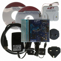
DEV KIT F220/221/226/230/231/236
Manufacturer
Silicon Laboratories Inc
Type
MCUr
Datasheet
1.C8051F226DK.pdf
(146 pages)
Specifications of C8051F226DK
Contents
Evaluation Board, Power Supply, USB Cables, Adapter and Documentation
Processor To Be Evaluated
C8051F22x and C8051F23x
Interface Type
USB
Silicon Manufacturer
Silicon Labs
Core Architecture
8051
Silicon Core Number
C8051F226
Silicon Family Name
C8051F2xx
Lead Free Status / RoHS Status
Contains lead / RoHS non-compliant
For Use With/related Products
C8051F220, 221, 226, 230, 231, 236
Lead Free Status / Rohs Status
Lead free / RoHS Compliant
Other names
336-1241


C8051F2xx
6.
Description
The ADC subsystem for the C8051F206 consists of configurable analog multiplexer (AMUX), a program-
mable gain amplifier (PGA), and a 100ksps, 12-bit successive-approximation-register ADC with integrated
track-and-hold and programmable window detector (see Figure 6.1). The AMUX, PGA, Data Conversion
Modes, and Window Detector are all configurable under software control via the Special Function Regis-
ter's shown in Figure 6.1. The ADC subsystem (ADC, track-and-hold and PGA) is enabled only when the
ADCEN bit in the ADC Control register (ADC0CN, Figure 6.5) is set to 1. The ADC subsystem is in low
power shutdown when this bit is 0.
6.1.
Any external port pin (ports 0-3) may be selected via software. The AMX0SL SFR is used to select the
desired analog input pin. (See SFR Definition 5.1). When the AMUX is enabled, the user selects which
port is to be used (bits PRTSL0–1), and then the pin in the selected port (bits PINSL0–2) to be the analog
input.
The PGA amplifies the AMUX output signal by an amount determined by the states of the AMPGN2–0 bits
in the ADC Configuration register, ADC0CF (SFR Definition 5.2). The PGA can be software-programmed
for gains of 0.5, 1, 2, 4, 8 or 16. It defaults to a gain of 1 on reset.
40
AIN31
AIN0
port pin may be configured
ADC (12-Bit, C8051F206 Only)
AIN0-31 are port 0-3
pins -- any external
as an analog input
Analog Multiplexer and PGA
Figure 6.1. 12-Bit ADC Functional Block Diagram
ADC0GTH
32-to-1
AMUX
AMX0SL
X
GND
ADC0GTL
+
-
GND
VDD
ADCEN
ADC0CF
Rev. 1.6
ADC0LTH
ADC
12-Bit
VDD
SAR
ADC0CN
VDD
ADC0LTL
12
VREF
24
12
T2 OV
Comp
Dig
ADWINT
Related parts for C8051F226DK
Image
Part Number
Description
Manufacturer
Datasheet
Request
R

Part Number:
Description:
SMD/C°/SINGLE-ENDED OUTPUT SILICON OSCILLATOR
Manufacturer:
Silicon Laboratories Inc
Part Number:
Description:
Manufacturer:
Silicon Laboratories Inc
Datasheet:
Part Number:
Description:
N/A N/A/SI4010 AES KEYFOB DEMO WITH LCD RX
Manufacturer:
Silicon Laboratories Inc
Datasheet:
Part Number:
Description:
N/A N/A/SI4010 SIMPLIFIED KEY FOB DEMO WITH LED RX
Manufacturer:
Silicon Laboratories Inc
Datasheet:
Part Number:
Description:
N/A/-40 TO 85 OC/EZLINK MODULE; F930/4432 HIGH BAND (REV E/B1)
Manufacturer:
Silicon Laboratories Inc
Part Number:
Description:
EZLink Module; F930/4432 Low Band (rev e/B1)
Manufacturer:
Silicon Laboratories Inc
Part Number:
Description:
I°/4460 10 DBM RADIO TEST CARD 434 MHZ
Manufacturer:
Silicon Laboratories Inc
Part Number:
Description:
I°/4461 14 DBM RADIO TEST CARD 868 MHZ
Manufacturer:
Silicon Laboratories Inc
Part Number:
Description:
I°/4463 20 DBM RFSWITCH RADIO TEST CARD 460 MHZ
Manufacturer:
Silicon Laboratories Inc
Part Number:
Description:
I°/4463 20 DBM RADIO TEST CARD 868 MHZ
Manufacturer:
Silicon Laboratories Inc
Part Number:
Description:
I°/4463 27 DBM RADIO TEST CARD 868 MHZ
Manufacturer:
Silicon Laboratories Inc
Part Number:
Description:
I°/4463 SKYWORKS 30 DBM RADIO TEST CARD 915 MHZ
Manufacturer:
Silicon Laboratories Inc
Part Number:
Description:
N/A N/A/-40 TO 85 OC/4463 RFMD 30 DBM RADIO TEST CARD 915 MHZ
Manufacturer:
Silicon Laboratories Inc
Part Number:
Description:
I°/4463 20 DBM RADIO TEST CARD 169 MHZ
Manufacturer:
Silicon Laboratories Inc