C8051F226DK Silicon Laboratories Inc, C8051F226DK Datasheet - Page 88
C8051F226DK
Manufacturer Part Number
C8051F226DK
Description
DEV KIT F220/221/226/230/231/236
Manufacturer
Silicon Laboratories Inc
Type
MCUr
Datasheet
1.C8051F226DK.pdf
(146 pages)
Specifications of C8051F226DK
Contents
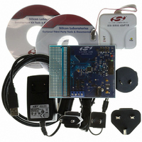
Evaluation Board, Power Supply, USB Cables, Adapter and Documentation
Processor To Be Evaluated
C8051F22x and C8051F23x
Interface Type
USB
Silicon Manufacturer
Silicon Labs
Core Architecture
8051
Silicon Core Number
C8051F226
Silicon Family Name
C8051F2xx
Lead Free Status / RoHS Status
Contains lead / RoHS non-compliant
For Use With/related Products
C8051F220, 221, 226, 230, 231, 236
Lead Free Status / Rohs Status
Lead free / RoHS Compliant
Other names
336-1241


C8051F2xx
The Flash Access Limit security feature protects proprietary program code and data from being read by
software running on the CIP-51. This feature provides support for OEMs that wish to program the MCU
with proprietary value-added firmware before distribution. The value-added firmware can be protected
while allowing additional code to be programmed in remaining program memory space later.
The Software Read Limit (SRL) is a 16-bit address that establishes two logical partitions in the program
memory space. The first is an upper partition consisting of all the program memory locations at or above
the SRL address, and the second is a lower partition consisting of all the program memory locations start-
ing at 0x0000 up to (but excluding) the SRL address. Software in the upper partition can execute code in
the lower partition, but is prohibited from reading locations in the lower partition using the MOVC instruc-
tion. (Executing a MOVC instruction from the upper partition with a source address in the lower partition
will always return a data value of 0x00.) Software running in the lower partition can access locations in
both the upper and lower partition without restriction.
The Value-added firmware should be placed in the lower partition. On reset, control is passed to the value-
added firmware via the reset vector. Once the value-added firmware completes its initial execution, it
branches to a predetermined location in the upper partition. If entry points are published, software running
in the upper partition may execute program code in the lower partition, but it cannot read the contents of
the lower partition. Parameters may be passed to the program code running in the lower partition either
through the typical method of placing them on the stack or in registers before the call or by placing them in
prescribed memory locations in the upper partition.
The SRL address is specified using the contents of the Flash Access Register. The 16-bit SRL address is
calculated as 0xNN00, where NN is the contents of the SRL Security Register. Thus, the SRL can be
located on 256-byte boundaries anywhere in program memory space. However, the 512-byte erase sector
size essentially requires that a 512 boundary be used. The contents of a non-initialized SRL security byte
is 0x00, thereby setting the SRL address to 0x0000 and allowing read access to all locations in program
memory space by default.
88
Bits7–2: UNUSED. Read = 000000b, Write = don't care.
Bit1:
Bit0:
R/W
Bit7
-
PSEE: Program Store Erase Enable.
Setting this bit allows an entire page of the Flash program memory to be erased (provided
the PSWE bit is set to '1'). After setting this bit, a write to Flash memory using the MOVX
instruction will erase the entire page that contains the location addressed by the MOVX
instruction. The value of the data byte written does not matter.
0: Flash program memory erasure disabled.
1: Flash program memory erasure enabled.
PSWE: Program Store Write Enable.
Setting this bit allows writing a byte of data to the Flash program memory using the MOVX
instruction. The location must be erased before writing data.
0: Write to Flash program memory disabled.
1: Write to Flash program memory enabled.
R/W
Bit6
SFR Definition 10.1. PSCTL: Program Store RW Control
-
R/W
Bit5
-
R/W
Bit4
-
Rev. 1.6
R/W
Bit3
-
R/W
Bit2
-
PSEE
R/W
Bit1
PSWE
R/W
Bit0
SFR Address:
Reset Value
00000000
0x8F
Related parts for C8051F226DK
Image
Part Number
Description
Manufacturer
Datasheet
Request
R

Part Number:
Description:
SMD/C°/SINGLE-ENDED OUTPUT SILICON OSCILLATOR
Manufacturer:
Silicon Laboratories Inc
Part Number:
Description:
Manufacturer:
Silicon Laboratories Inc
Datasheet:
Part Number:
Description:
N/A N/A/SI4010 AES KEYFOB DEMO WITH LCD RX
Manufacturer:
Silicon Laboratories Inc
Datasheet:
Part Number:
Description:
N/A N/A/SI4010 SIMPLIFIED KEY FOB DEMO WITH LED RX
Manufacturer:
Silicon Laboratories Inc
Datasheet:
Part Number:
Description:
N/A/-40 TO 85 OC/EZLINK MODULE; F930/4432 HIGH BAND (REV E/B1)
Manufacturer:
Silicon Laboratories Inc
Part Number:
Description:
EZLink Module; F930/4432 Low Band (rev e/B1)
Manufacturer:
Silicon Laboratories Inc
Part Number:
Description:
I°/4460 10 DBM RADIO TEST CARD 434 MHZ
Manufacturer:
Silicon Laboratories Inc
Part Number:
Description:
I°/4461 14 DBM RADIO TEST CARD 868 MHZ
Manufacturer:
Silicon Laboratories Inc
Part Number:
Description:
I°/4463 20 DBM RFSWITCH RADIO TEST CARD 460 MHZ
Manufacturer:
Silicon Laboratories Inc
Part Number:
Description:
I°/4463 20 DBM RADIO TEST CARD 868 MHZ
Manufacturer:
Silicon Laboratories Inc
Part Number:
Description:
I°/4463 27 DBM RADIO TEST CARD 868 MHZ
Manufacturer:
Silicon Laboratories Inc
Part Number:
Description:
I°/4463 SKYWORKS 30 DBM RADIO TEST CARD 915 MHZ
Manufacturer:
Silicon Laboratories Inc
Part Number:
Description:
N/A N/A/-40 TO 85 OC/4463 RFMD 30 DBM RADIO TEST CARD 915 MHZ
Manufacturer:
Silicon Laboratories Inc
Part Number:
Description:
I°/4463 20 DBM RADIO TEST CARD 169 MHZ
Manufacturer:
Silicon Laboratories Inc