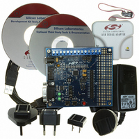
C8051F350DK Silicon Laboratories Inc, C8051F350DK Datasheet - Page 7

C8051F350DK
Manufacturer Part Number
C8051F350DK
Description
DEV KIT FOR F350/351/352/353
Manufacturer
Silicon Laboratories Inc
Type
MCUr
Specifications of C8051F350DK
Contents
Evaluation Board, Power Supply, USB Cables, Adapter and Documentation
Processor To Be Evaluated
C8051F35x
Interface Type
USB
Silicon Manufacturer
Silicon Labs
Core Architecture
8051
Silicon Core Number
C8051F350
Silicon Family Name
C8051F35x
Lead Free Status / RoHS Status
Contains lead / RoHS non-compliant
For Use With/related Products
C8051F350, 351, 352, 353
Lead Free Status / Rohs Status
Lead free / RoHS Compliant
Other names
336-1083
Available stocks
Company
Part Number
Manufacturer
Quantity
Price
Company:
Part Number:
C8051F350DK
Manufacturer:
SiliconL
Quantity:
8
6.3. Expansion I/O Connector (J1)
The 34-pin Expansion I/O connector J1 provides access to all signal pins of the C8051F350 device. Pins for V
GND as well as pins for VDDA and AGND are also available. A small through-hole prototyping area is also provided.
All I/O signals routed to connector J1 are also routed to through-hole connection points between J1 and the prototyp-
ing area (see Figure 2 on page 5). Each connection point is labeled indicating the signal available at the connection
point. See Table 2 for a list of pin descriptions for J1.
6.4. Target Board DEBUG Interface (J4)
The DEBUG connector (J4) provides access to the DEBUG (C2) pins of the C8051F350. It is used to connect the
Serial Adapter or the USB Debug Adapter to the target board for in-circuit debugging and Flash programming.
Table 3 shows the DEBUG pin definitions.
6.5. Serial Interface (J5)
A RS232 transceiver circuit and DB-9 (J5) connector are provided on the target board to facilitate serial connec-
tions to UART0 of the C8051F350. The TX, RX, RTS and CTS signals of UART0 may be connected to the DB-9
connector and transceiver by installing shorting blocks on header J3.
J3[7–8]
J3[9–10] - Install shorting block to connect UART0 RX (P0.5) to transceiver.
J3[11–12] - Install shorting block to connect UART0 RTS (P1.4) to transceiver.
J3[13–14] - Install shorting block to connect UART0 CTS (P1.5) to transceiver.
Pin #
10
11
1
2
3
4
5
6
7
8
9
- Install shorting block to connect UART0 TX (P0.4) to transceiver.
Description
GND
P0.0
P0.1
P0.2
P0.3
P0.4
P0.5
P0.6
P0.7
P1.0
P1.1
V
DD
Table 3. DEBUG Connector Pin Descriptions
2, 3, 9
Pin #
10
1
4
5
6
7
8
Table 2. J1 Pin Descriptions
Pin #
13
14
15
16
17
18
19
20
21
22
23
24
+3 VD (+3.3 VDC)
Rev. 0.3
Description
Not Connected
GND (Ground)
P1.6/IDAC0
P1.7/IDAC1
Description
/RST (Reset)
USB Power
AGND
AGND
AIN0
AIN1
AIN2
P1.2
P1.3
P1.4
P1.5
P2.0
C2CK
C2D
P3.0
Pin #
25
26
27
28
29
30
31
32
33
34
-
-
C8051F35x-DK
Description
VREF+
VREF–
AGND
VDDA
/RST
AIN3
AIN4
AIN5
AIN6
AIN7
-
-
DD
and
7


