C8051F350DK Silicon Laboratories Inc, C8051F350DK Datasheet - Page 8
C8051F350DK
Manufacturer Part Number
C8051F350DK
Description
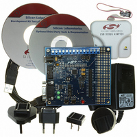
DEV KIT FOR F350/351/352/353
Manufacturer
Silicon Laboratories Inc
Type
MCUr
Specifications of C8051F350DK
Contents
Evaluation Board, Power Supply, USB Cables, Adapter and Documentation
Processor To Be Evaluated
C8051F35x
Interface Type
USB
Silicon Manufacturer
Silicon Labs
Core Architecture
8051
Silicon Core Number
C8051F350
Silicon Family Name
C8051F35x
Lead Free Status / RoHS Status
Contains lead / RoHS non-compliant
For Use With/related Products
C8051F350, 351, 352, 353
Lead Free Status / Rohs Status
Lead free / RoHS Compliant
Other names
336-1083
Available stocks
Company
Part Number
Manufacturer
Quantity
Price
Company:

Part Number:
C8051F350DK
Manufacturer:
SiliconL
Quantity:
8


C8051F35x-DK
6.6. Analog I/O (J6)
Many of the C8051F350 target device’s port pins are connected to the J6 terminal block. Connections for VDDA,
AGND, ADC external voltage refences, IDAC outputs and ADC inputs are available. Refer to Table 4 for the J6 ter-
minal block connections.
6.7. IDAC Connectors (J7, J11)
The C8051F350 target board also features two Current-to-Voltage 1 KΩ load resistors that may be connected to
the 10-bit current-mode Digital-to-Analog Converters (IDACs) on port pins P1.6 and P1.7. Install a shorting block
on J7 to connect the IDAC0/P1.6 pin of the target device to a load resistor. Install a second shorting block on J11 to
connect the IDAC1/P1.7 pin of the target device to a load resistor. The IDAC signals are then routed to the J1 and
J6 connectors.
6.8. USB Debug Adapter Target Board Power Connector (J8)
The USB Debug Adapter includes a connection to provide power to the target board. This connection is routed
from J4[10] to J8[1]. Place a shorting block at header J8[2-3] to power the board directly from an ac/dc power
adapter. Place a shorting block at header J8[1-2] to power the board from the USB Debug Adapter. Please note
that the second option is not supported with either the EC1 or EC2 Serial Adapters.
6.9. Thermistor Connector Block (J12)
A thermistor circuit is included on the board which allows for a ratiometric measurement of the included thermistor.
To use the circuit, remove the shorting blocks on the IDAC headers (J7, J11) and the External Voltage Reference
headers (J13, J14). Next, connect all of the signals on the thermistor connector block (J12). Software on the chip
can be written to use IDAC0 as a reference current source for the circuit. The current creates a voltage across R27
which is used as an external Voltage Reference input, while the voltage across the thermistor (R26) can be mea-
sured by connecting AIN0.0 to the AIN+ ADC input, and AIN0.1 to the AIN- ADC input.
6.10. External Voltage Reference (J13, J14)
A precision 2.5V voltage reference source is also included on the C8051F350 target board. To use this circuit as a
reference source for the ADC, place shorting block on headers J13 and J14. Note that software on the device
should be configured to use an external reference when using this configuration. When using the internal (on-chip)
reference source, headers J13 and J14 should be left open.
8
Pin #
Table 4. J6 Terminal Block Pin Descriptions
1
2
3
4
5
6
7
Description
VREF+
VREF–
IDAC0
IDAC1
AIN0
AIN1
AIN2
Rev. 0.3
Pin #
10
12
13
14
11
8
9
Description
AGND
VDDA
AIN3
AIN4
AIN5
AIN6
AIN7
Related parts for C8051F350DK
Image
Part Number
Description
Manufacturer
Datasheet
Request
R

Part Number:
Description:
SMD/C°/SINGLE-ENDED OUTPUT SILICON OSCILLATOR
Manufacturer:
Silicon Laboratories Inc
Part Number:
Description:
Manufacturer:
Silicon Laboratories Inc
Datasheet:
Part Number:
Description:
N/A N/A/SI4010 AES KEYFOB DEMO WITH LCD RX
Manufacturer:
Silicon Laboratories Inc
Datasheet:
Part Number:
Description:
N/A N/A/SI4010 SIMPLIFIED KEY FOB DEMO WITH LED RX
Manufacturer:
Silicon Laboratories Inc
Datasheet:
Part Number:
Description:
N/A/-40 TO 85 OC/EZLINK MODULE; F930/4432 HIGH BAND (REV E/B1)
Manufacturer:
Silicon Laboratories Inc
Part Number:
Description:
EZLink Module; F930/4432 Low Band (rev e/B1)
Manufacturer:
Silicon Laboratories Inc
Part Number:
Description:
I°/4460 10 DBM RADIO TEST CARD 434 MHZ
Manufacturer:
Silicon Laboratories Inc
Part Number:
Description:
I°/4461 14 DBM RADIO TEST CARD 868 MHZ
Manufacturer:
Silicon Laboratories Inc
Part Number:
Description:
I°/4463 20 DBM RFSWITCH RADIO TEST CARD 460 MHZ
Manufacturer:
Silicon Laboratories Inc
Part Number:
Description:
I°/4463 20 DBM RADIO TEST CARD 868 MHZ
Manufacturer:
Silicon Laboratories Inc
Part Number:
Description:
I°/4463 27 DBM RADIO TEST CARD 868 MHZ
Manufacturer:
Silicon Laboratories Inc
Part Number:
Description:
I°/4463 SKYWORKS 30 DBM RADIO TEST CARD 915 MHZ
Manufacturer:
Silicon Laboratories Inc
Part Number:
Description:
N/A N/A/-40 TO 85 OC/4463 RFMD 30 DBM RADIO TEST CARD 915 MHZ
Manufacturer:
Silicon Laboratories Inc
Part Number:
Description:
I°/4463 20 DBM RADIO TEST CARD 169 MHZ
Manufacturer:
Silicon Laboratories Inc