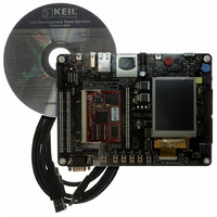
MCB2470 Keil, MCB2470 Datasheet
MCB2470
Specifications of MCB2470


Related parts for MCB2470


MCB2470 Summary of contents
Page 1
LPC2478 Single-chip 16-bit/32-bit micro; 512 kB Flash, Ethernet, CAN, LCD, USB 2.0 Device/Host/OTG, External memory interface Rev. 01 — 9 February 2007 1. General description NXP Semiconductor designed the LPC2478 microcontroller, powered by the ARM7TDMI-S core highly ...
Page 2
NXP Semiconductors LCD controller, supporting both Super-Twisted Nematic (STN) and Thin-Film Transistors (TFT) displays. Dedicated DMA controller. Selectable display resolution (up to 1024 × 768 pixels). Supports up to 24-bit true-color mode. Dual Advanced High-performance Bus (AHB) system allows simultaneous ...
Page 3
NXP Semiconductors Processor wake-up from Power-down mode via any interrupt able to operate during Power-down mode (includes external interrupts, RTC interrupt, USB activity, Ethernet wake-up interrupt, CAN bus activity, PORT0/2 pin interrupt). Two independent power domains allow fine tuning of ...
Page 4
NXP Semiconductors 4.1 Ordering options Table 2. Ordering options Type number Flash SRAM (kB) (kB) LPC2478FBD208 512 64 16 LPC2478FET208 512 64 16 LPC2478_1 Preliminary data sheet External Ethernet USB bus Full MII/ 32-bit RMII 16 2 ...
Page 5
NXP Semiconductors 5. Block diagram LPC2478 P0, P1, P2 P3, P4 SRAM HIGH-SPEED GPI/O 160 PINS TOTAL AHB2 16 kB ETHERNET SRAM MII/RMII MAC WITH DMA EINT3 to EINT0 EXTERNAL INTERRUPTS P0 × CAP0/CAP1/ CAPTURE/COMPARE CAP2/CAP3 ...
Page 6
NXP Semiconductors 6. Pinning information 6.1 Pinning Fig 2. LPC2478 pinning LQFP208 package Fig 3. LPC2478 pinning TFBGA208 package Table 3. Pin allocation table Pin Symbol Pin Symbol Row A 1 P3[27]/D27/ 2 CAP1[0]/PWM1[4] 5 P1[4]/ENET_TX_EN 6 9 P1[17]/ENET_MDIO 10 ...
Page 7
NXP Semiconductors Table 3. Pin allocation table …continued Pin Symbol Pin Symbol 13 P3[20]/D20/ 14 PWM0[5]/DSR1 17 P1[5]/ENET_TX_ER/ MCIPWR/PWM0[3] Row B 1 P3[2]/ P1[1]/ENET_TXD1 6 9 P4[25]/ DD(3V3) 17 P2[0]/PWM1[1]/TXD1/ TRACECLK/LCDPWR Row C 1 ...
Page 8
NXP Semiconductors Table 3. Pin allocation table …continued Pin Symbol Pin Symbol 14 P4[11]/A11 15 Row G 1 P3[5]/ Row H 1 P0[23]/AD0[0]/ 2 I2SRX_CLK/CAP3[ SSIO Row J 1 P3[6]/ P0[16]/RXD1/ ...
Page 9
NXP Semiconductors Table 3. Pin allocation table …continued Pin Symbol Pin Symbol 9 P1[23]/USB_RX_DP1/ 10 LCD[9]/LCD[13]/ PWM1[4]/MISO0 13 P2[15]/CS3/ 14 CAP2[1]/SCL1 17 V DD(3V3) Row R 1 P0[12]/USB_PPWR2/ 2 MISO1/AD0[6] 5 P3[24]/D24/ 6 CAP0[1]/PWM1[ SSIO 13 P2[17]/RAS ...
Page 10
NXP Semiconductors 6.2 Pin description Table 4. Pin description Symbol Pin Ball P0[0] to P0[31] [1] P0[0]/RD1/TXD3/ 94 U15 SDA1 [1] P0[1]/TD1/RXD3/ 96 T14 SCL1 [1] [1] P0[2]/TXD0 202 C4 [1] [1] P0[3]/RXD0 204 D6 [1] P0[4]/I2SRX_CLK/ 168 B12 LCD[0]/RD2/ ...
Page 11
NXP Semiconductors Table 4. Pin description …continued Symbol Pin Ball [1] P0[7]/I2STX_CLK/ 162 C13 LCD[9]/SCK1/ MAT2[1] [1] P0[8]/I2STX_WS/ 160 A15 LCD[16]/ MISO1/MAT2[2] [1] P0[9]/I2STX_SDA/ 158 C14 LCD[17]/ MOSI1/MAT2[3] [1] P0[10]/TXD2/ 98 T15 SDA2/MAT3[0] [1] P0[11]/RXD2/ 100 R14 SCL2/MAT3[1] [2] [2] ...
Page 12
NXP Semiconductors Table 4. Pin description …continued Symbol Pin Ball [1] [1] P0[14 USB_HSTEN2/ USB_CONNECT2/ SSEL1 [1] [1] P0[15]/TXD1/ 128 J16 SCK0/SCK [1] [1] P0[16]/RXD1/ 130 J14 SSEL0/SSEL [1] P0[17]/CTS1/ 126 K17 MISO0/MISO [1] P0[18]/DCD1/ 124 K15 MOSI0/MOSI ...
Page 13
NXP Semiconductors Table 4. Pin description …continued Symbol Pin Ball [2] [2] P0[23]/AD0[0 I2SRX_CLK/ CAP3[0] [2] [2] P0[24]/AD0[1 I2SRX_WS/ CAP3[1] [2] [2] P0[25]/AD0[2 I2SRX_SDA/ TXD3 [2][3] [2][3] P0[26]/AD0[3 AOUT/RXD3 [4] [4] P0[27]/SDA0 ...
Page 14
NXP Semiconductors Table 4. Pin description …continued Symbol Pin Ball [1] P1[3]/ 177 A10 ENET_TXD3/ MCICMD/ PWM0[2] [1] [1] P1[4]/ 192 A5 ENET_TX_EN [1] P1[5]/ 156 A17 ENET_TX_ER/ MCIPWR/ PWM0[3] [1] P1[6]/ 171 B11 ENET_TX_CLK/ MCIDAT0/ PWM0[4] [1] P1[7]/ 153 ...
Page 15
NXP Semiconductors Table 4. Pin description …continued Symbol Pin Ball [1] P1[16]/ 180 D10 ENET_MDC [1] [1] P1[17]/ 178 A9 ENET_MDIO [1] [1] P1[18 USB_UP_LED1/ PWM1[1]/CAP1[0] [1] [1] P1[19 USB_TX_E1/ USB_PPWR1/ CAP1[1] [1] [1] P1[20]/ 70 ...
Page 16
NXP Semiconductors Table 4. Pin description …continued Symbol Pin Ball [1] P1[25]/USB_LS1/ 80 T10 LCD[11]/LCD[15]/ USB_HSTEN1/ MAT1[1] [1] P1[26]/ 82 R10 USB_SSPND1/ LCD[12]/LCD[20]/ PWM1[6]/ CAP0[0] [1] P1[27]/USB_INT1/ 88 T12 LCD[13]/LCD[21]/ USB_OVRCR1/ CAP0[1] [1] P1[28]/USB_SCL1/ 90 T13 LCD[14]/LCD[22]/ PCAP1[0]/ MAT0[0] [1] ...
Page 17
NXP Semiconductors Table 4. Pin description …continued Symbol Pin Ball [1] P2[0]/PWM1[1]/ 154 B17 TXD1/TRACECLK/ LCDPWR [1] P2[1]/PWM1[2]/ 152 E14 RXD1/PIPESTAT0/ LCDLE [1] P2[2]/PWM1[3]/ 150 D15 CTS1/PIPESTAT1/ LCDCP [1] P2[3]/PWM1[4]/ 144 E16 DCD1/PIPESTAT2/ LCDFP [1] P2[4]/PWM1[5]/ 142 D17 DSR1/ TRACESYNC/ ...
Page 18
NXP Semiconductors Table 4. Pin description …continued Symbol Pin Ball [1] P2[8]/TD2/TXD2/ 134 H15 TRACEPKT3/ LCD[2]/LCD[6] [1] P2[9]/ 132 H16 USB_CONNECT1/ RXD2/EXTIN0/ LCD[3]/LCD[7] [6] P2[10]/EINT0 110 N15 [6] P2[11]/EINT1/ 108 T17 LCDCLKIN/ MCIDAT1/ I2STX_CLK [6] P2[12]/EINT2/ 106 N14 LCD[4]/LCD[3]/ LCD[8]/LCD[18]/ ...
Page 19
NXP Semiconductors Table 4. Pin description …continued Symbol Pin Ball [1] P2[16]/CAS 87 R11 [1] P2[17]/RAS 95 R13 [1] [1] P2[18 CLKOUT0 [1] [1] P2[19 CLKOUT1 [1] [1] P2[20]/DYCS0 73 T8 [1] P2[21]/DYCS1 81 U11 [1] ...
Page 20
NXP Semiconductors Table 4. Pin description …continued Symbol Pin Ball [1] [1] P2[31 DQMOUT3/ MAT3[3]/SCL2 P3[0] to P3[31] [1] [1] P3[0]/D0 197 B4 [1] [1] P3[1]/D1 201 B3 [1] [1] P3[2]/D2 207 B1 [1] [1] P3[3]/ ...
Page 21
NXP Semiconductors Table 4. Pin description …continued Symbol Pin Ball [1] P3[16]/D16/ 137 F17 PWM0[1]/TXD1 [1] P3[17]/D17/ 143 F15 PWM0[2]/RXD1 [1] P3[18]/D18/ 151 C15 PWM0[3]/CTS1 [1] P3[19]/D19/ 161 B14 PWM0[4]/DCD1 [1] P3[20]/D20/ 167 A13 PWM0[5]/DSR1 [1] P3[21]/D21/ 175 C10 PWM0[6]/DTR1 ...
Page 22
NXP Semiconductors Table 4. Pin description …continued Symbol Pin Ball [1] [1] P3[26]/D26 MAT0[1]/ PWM1[3] [1] [1] P3[27]/D27/ 203 A1 CAP1[0]/ PWM1[4] [1] [1] P3[28]/D28 CAP1[1]/ PWM1[5] [1] [1] P3[29]/D29 MAT1[0]/ PWM1[6] [1] [1] ...
Page 23
NXP Semiconductors Table 4. Pin description …continued Symbol Pin Ball [1] P4[7]/A7 121 L16 [1] [1] P4[8]/A8 127 J17 [1] P4[9]/A9 131 H17 [1] P4[10]/A10 135 G17 [1] P4[11]/A11 145 F14 [1] P4[12]/A12 149 C16 [1] P4[13]/A13 155 B16 [1] ...
Page 24
NXP Semiconductors Table 4. Pin description …continued Symbol Pin Ball [1] [1] P4[23]/A23/ 129 J15 RXD2/MOSI1 [1] [1] P4[24]/OE 183 B8 [1] [1] P4[25]/WE 179 B9 [1] P4[26]/BLS0 119 L15 [1] P4[27]/BLS1 139 G15 [1] P4[28]/BLS2/ 170 C11 MAT2[0]/LCD[6]/ LCD[10]/LCD[2]/ ...
Page 25
NXP Semiconductors Table 4. Pin description …continued Symbol Pin Ball [7] [7] RESET 35 M2 [8] [8] XTAL1 44 M4 [8] [8] XTAL2 46 N4 [8] [8] RTCX1 34 K2 [8] [8] RTCX2 33, 63, L3, T5, ...
Page 26
NXP Semiconductors [9] Pad provides special analog functionality. [10] Pad provides special analog functionality. [11] Pad provides special analog functionality. [12] Pad provides special analog functionality. [13] Pad provides special analog functionality. [14] Pad provides special analog functionality. 2 [15] ...
Page 27
NXP Semiconductors Pipeline techniques are employed so that all parts of the processing and memory systems can operate continuously. Typically, while one instruction is being executed, its successor is being decoded, and a third instruction is being fetched from memory. ...
Page 28
NXP Semiconductors Table 5. Address range General use 0x0000 0000 to 0x3FFF FFFF 0x4000 0000 to 0x7FFF FFFF 0x8000 0000 to 0xDFFF FFFF 0xE000 0000 to 0xEFFF FFFF 0xF000 0000 to 0xFFFF FFFF LPC2478_1 Preliminary data sheet LPC2478 memory usage ...
Page 29
NXP Semiconductors 4.0 GB 3.75 GB 3.5 GB 3.0 GB 2.0 GB 1.0 GB 0.0 GB Fig 4. LPC2478 memory map 7.5 Interrupt controller The ARM processor core has two interrupt inputs called Interrupt Request (IRQ) and Fast Interrupt Request ...
Page 30
NXP Semiconductors service routine can simply start dealing with that device. But if more than one request is assigned to the FIQ class, the FIQ service routine can read a word from the VIC that identifies which FIQ source(s) is ...
Page 31
NXP Semiconductors – Asynchronous page mode read – Programmable Wait States – Bus turnaround delay – Output enable and write enable delays – Extended wait • Four chip selects for synchronous memory and four chip selects for static memory devices ...
Page 32
NXP Semiconductors • 32-bit AHB master bus width. • Incrementing or non-incrementing addressing for source and destination. • Programmable DMA burst size. The DMA burst size can be programmed to more efficiently transfer data. Usually the burst size is set ...
Page 33
NXP Semiconductors 7.10 LCD controller The LCD controller provides all of the necessary control signals to interface directly to a variety of color and monochrome LCD panels. Both STN (single and dual panel) and TFT panels can be operated. The ...
Page 34
NXP Semiconductors The Ethernet block and the CPU share a dedicated AHB subsystem that is used to access the Ethernet SRAM for Ethernet data, control, and status information. All other AHB traffic in the LPC2478 takes place on a different ...
Page 35
NXP Semiconductors 7.12 USB interface The Universal Serial Bus (USB 4-wire bus that supports communication between a host and one or more (up to 127) peripherals. The host controller allocates the USB bandwidth to attached devices through a ...
Page 36
NXP Semiconductors 7.12.3 USB OTG controller USB OTG (On-The-Go supplement to the USB 2.0 specification that augments the capability of existing mobile devices and USB peripherals by adding host functionality for connection to USB peripherals. The OTG controller ...
Page 37
NXP Semiconductors 7.14 10-bit ADC The LPC2478 contains one ADC single 10-bit successive approximation ADC with eight channels. 7.14.1 Features • 10-bit successive approximation ADC • Input multiplexing among 8 pins • Power-down mode • Measurement range ...
Page 38
NXP Semiconductors • UART3 includes an IrDA mode to support infrared communication. 7.17 SPI serial I/O controller The LPC2478 contains one SPI controller. SPI is a full duplex serial interface designed to handle multiple masters and slaves connected to a ...
Page 39
NXP Semiconductors • Conforms to Multimedia Card Specification v2.11. • Conforms to Secure Digital Memory Card Physical Layer Specification, v0.96. • Can be used as a multimedia card bus or a secure digital memory card bus host. The SD/MMC can ...
Page 40
NXP Semiconductors 7.21.1 Features • The interface has separate input/output channels each of which can operate in master or slave mode. • Capable of handling 8-bit, 16-bit, and 32-bit word sizes. • Mono and stereo audio data supported. • The ...
Page 41
NXP Semiconductors 7.23 Pulse width modulator The PWM is based on the standard Timer block and inherits all of its features, although only the PWM function is pinned out on the LPC2478. The Timer is designed to count cycles of ...
Page 42
NXP Semiconductors • Pulse period and width can be any number of timer counts. This allows complete flexibility in the trade-off between resolution and repetition rate. All PWM outputs will occur at the same repetition rate. • Double edge controlled ...
Page 43
NXP Semiconductors 7.25.1 Features • Measures the passage of time to maintain a calendar and clock. • Ultra low power design to support battery powered systems. • Provides Seconds, Minutes, Hours, Day of Month, Month, Year, Day of Week, and ...
Page 44
NXP Semiconductors 7.26.1.3 RTC oscillator The RTC oscillator can be used as the clock source for the RTC and/or the WDT. Also, the RTC oscillator can be used to drive the PLL and the CPU. 7.26.2 PLL The PLL accepts ...
Page 45
NXP Semiconductors PLL values, and/or altering the CPU clock divider value. This allows a trade-off of power versus processing speed based on application requirements. In addition, Peripheral power control allows shutting down the clocks to individual on-chip peripherals, allowing fine ...
Page 46
NXP Semiconductors 7.26.4.4 Power domains The LPC2478 provides two independent power domains that allow the bulk of the device to have power removed while maintaining operation of the RTC and the Battery RAM. On the LPC2478, I/O pads are powered ...
Page 47
NXP Semiconductors The second stage of low-voltage detection asserts Reset to inactivate the LPC2478 when the voltage on the V flash as operation of the various elements of the chip would otherwise become unreliable due to low voltage. The BOD ...
Page 48
NXP Semiconductors 7.27.6 Memory mapping control The memory mapping control alters the mapping of the interrupt vectors that appear at the beginning at address 0x0000 0000. Vectors may be mapped to the bottom of the Boot ROM, the SRAM, or ...
Page 49
NXP Semiconductors 7.28.3 RealMonitor RealMonitor is a configurable software module, developed by ARM Inc., which enables real-time debug lightweight debug monitor that runs in the background while users debug their foreground application. It communicates with the host ...
Page 50
NXP Semiconductors 8. Limiting values Table 6. Limiting values In accordance with the Absolute Maximum Rating System (IEC 60134). Symbol Parameter V supply voltage (3.3 V) DD(3V3) V DC-to-DC converter supply voltage DD(DCDC)(3V3) (3 analog 3.3 V pad ...
Page 51
NXP Semiconductors 9. Static characteristics Table 7. Static characteristics − ° ° +85 C for commercial applications, unless otherwise specified. amb Symbol Parameter V supply voltage (3.3 V) DD(3V3) V DC-to-DC converter DD(DCDC)(3V3) supply voltage ...
Page 52
NXP Semiconductors Table 7. Static characteristics …continued − ° ° +85 C for commercial applications, unless otherwise specified. amb Symbol Parameter I active mode DC-to-DC DD(DCDC)act(3V3) converter supply current (3 power-down mode DD(DCDC)pd(3V3) ...
Page 53
NXP Semiconductors Table 7. Static characteristics …continued − ° ° +85 C for commercial applications, unless otherwise specified. amb Symbol Parameter USB pins I OFF-state output OZ current V bus supply voltage BUS V differential ...
Page 54
NXP Semiconductors Table 8. ADC static characteristics − ° 2 3 +85 DDA amb Symbol Parameter V analog input voltage IA C analog input capacitance ia E differential linearity error ...
Page 55
NXP Semiconductors 1023 1022 1021 1020 1019 1018 7 code out offset error E O (1) Example of an actual transfer curve. (2) The ideal transfer curve. (3) Differential linearity ...
Page 56
NXP Semiconductors AD0[y] SAMPLE Fig 6. Suggested ADC interface - LPC2478 AD0[y] pin LPC2478_1 Preliminary data sheet LPC2XXX R vsi 20 kΩ AD0[ Rev. 01 — 9 February 2007 LPC2478 Fast communication chip V ...
Page 57
NXP Semiconductors 10. Dynamic characteristics Table 9. Dynamic characteristics of USB pins (full-speed) Ω pF 1 Symbol Parameter t rise time r t fall time f t differential ...
Page 58
NXP Semiconductors Table 11. External memory interface dynamic characteristics ° pF amb Symbol Parameter Common to read and write cycles t XCLK HIGH to address valid CHAV time t XCLK HIGH to ...
Page 59
NXP Semiconductors Table 11. External memory interface dynamic characteristics ° pF amb Symbol Parameter t BLS HIGH to data invalid BLSHDNV time t XCLK HIGH to data valid CHDV time t XCLK ...
Page 60
NXP Semiconductors 10.1 Timing XCLK CS addr data t CSLOEL OE Fig 7. External memory read access XCLK CS BLS/WE addr data OE Fig 8. External memory write access LPC2478_1 Preliminary data sheet t CSLAV OELAV t ...
Page 61
NXP Semiconductors V − 0 0.2V 0.2V DD 0.45 V Fig 9. External clock timing t PERIOD crossover point differential data lines differential data to n × t Fig 10. Differential data-to-EOP transition skew and EOP width LPC2478_1 ...
Page 62
NXP Semiconductors 11. Application information 11.1 LCD panel signal usage Table 13. LCD panel connections for STN single panel mode External pin 4-bit mono STN single panel LPC2478 pin LCD function used LCD[23 LCD[22 LCD[21] - ...
Page 63
NXP Semiconductors Table 14. LCD panel connections for STN dual panel mode External pin 4-bit mono STN dual panel LPC2478 pin LCD function used LCD[23 LCD[22 LCD[21 LCD[20 LCD[19 LCD[18] ...
Page 64
NXP Semiconductors Table 15. LCD panel connections for TFT panels External TFT 12 bit (4:4:4 mode) TFT 16 bit (5:6:5 mode) pin LPC2478 LCD pin used function [4] LCD[23] P1[29] BLUE3 [4] LCD[22] P1[28] BLUE2 [4] LCD[21] P1[27] BLUE1 [4] ...
Page 65
NXP Semiconductors 11.2 Suggested USB interface solutions LPC24XX Fig 11. LPC2478 USB interface on a self-powered device LPC24XX Fig 12. LPC2478 USB interface on a bus-powered device LPC2478_1 Preliminary data sheet V DD(3V3) USB_UP_LED USB_CONNECT soft-connect switch R1 1.5 kΩ ...
Page 66
NXP Semiconductors RSTOUT USB_SCL1 USB_SDA1 USB_INT1 USB_D+1 USB_D−1 USB_UP_LED1 LPC24XX USB_PPWR2 USB_OVRCR2 USB_PWRD2 USB_D+2 USB_D−2 USB_UP_LED2 Fig 13. LPC2478 USB OTG port configuration: USB port 1 OTG dual-role device, USB port 2 host LPC2478_1 Preliminary data sheet ...
Page 67
NXP Semiconductors RSTOUT USB_TX_E1 USB_TX_DP1 USB_TX_DM1 USB_RCV1 USB_RX_DP1 USB_RX_DM1 LPC24XX USB_SCL1 USB_SDA1 USB_INT1 USB_UP_LED1 Fig 14. LPC2478 USB OTG port configuration: VP_VM mode LPC2478_1 Preliminary data sheet V DD RESET_N OE_N/INT_N DAT_VP SE0_VM RCV ISP1301 ADR/PSW ...
Page 68
NXP Semiconductors USB_UP_LED1 USB_D+1 USB_D−1 USB_PWRD1 USB_OVRCR1 USB_PPWR1 LPC24XX USB_UP_LED2 USB_CONNECT2 USB_D+2 USB_D−2 V BUS Fig 15. LPC2478 USB OTG port configuration: USB port 2 device, USB port 1 host LPC2478_1 Preliminary data sheet Ω 33 Ω ...
Page 69
NXP Semiconductors USB_UP_LED1 USB_D+1 USB_D−1 USB_PWRD1 USB_OVRCR1 USB_PPWR1 LPC24XX USB_PPWR2 USB_OVRCR2 USB_PWRD2 USB_D+2 USB_D−2 USB_UP_LED2 Fig 16. LPC2478 USB OTG port configuration: USB port 1 host, USB port 2 host LPC2478_1 Preliminary data sheet Ω 33 Ω ...
Page 70
NXP Semiconductors 12. Package outline LQFP208; plastic low profile quad flat package; 208 leads; body 1 156 157 pin 1 index 208 DIMENSIONS (mm are the original ...
Page 71
NXP Semiconductors TFBGA208: plastic thin fine-pitch ball grid array package; 208 balls; body 0.7 mm ball A1 index area ...
Page 72
NXP Semiconductors 13. Abbreviations Table 16. Acronym list Acronym Description ADC Analog-to-Digital Converter AHB Advanced High-performance Bus AMBA Advanced Microcontroller Bus Architecture APB Advanced Peripheral Bus ATX Analog transceiver BLS Byte Lane Select BOD BrownOut Detection CAN Controller Area Network ...
Page 73
NXP Semiconductors 14. Revision history Table 17. Revision history Document ID Release date LPC2478_1 20070209 LPC2478_1 Preliminary data sheet Data sheet status Change notice Preliminary data sheet - Rev. 01 — 9 February 2007 LPC2478 Fast communication chip Supersedes - ...
Page 74
NXP Semiconductors 15. Legal information 15.1 Data sheet status [1][2] Document status Product status Objective [short] data sheet Development Preliminary [short] data sheet Qualification Product [short] data sheet Production [1] Please consult the most recently issued document before initiating or ...
Page 75
NXP Semiconductors 17. Contents 1 General description . . . . . . . . . . . . . . . . . . . . . . 1 2 Features . . . . . . . . ...
Page 76
NXP Semiconductors 15 Legal information 15.1 Data sheet status . . . . . . . . ...