MCB2470 Keil, MCB2470 Datasheet - Page 16
MCB2470
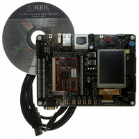
Manufacturer Part Number
MCB2470
Description
BOARD EVAL NXP LPC247X SERIES
Manufacturer
Keil
Type
MCUr
Specifications of MCB2470
Contents
Board, Cable, CD
For Use With/related Products
LPC2478
Lead Free Status / RoHS Status
Lead free / RoHS Compliant


NXP Semiconductors
Table 4.
LPC2478_1
Preliminary data sheet
Symbol
P1[25]/USB_LS1/
LCD[11]/LCD[15]/
USB_HSTEN1/
MAT1[1]
P1[26]/
USB_SSPND1/
LCD[12]/LCD[20]/
PWM1[6]/
CAP0[0]
P1[27]/USB_INT1/
LCD[13]/LCD[21]/
USB_OVRCR1/
CAP0[1]
P1[28]/USB_SCL1/
LCD[14]/LCD[22]/
PCAP1[0]/
MAT0[0]
P1[29]/USB_SDA1/
LCD[15]/LCD[23]/
PCAP1[1]/
MAT0[1]
P1[30]/
USB_PWRD2/
V
P1[31]/
USB_OVRCR2/
SCK1/AD0[5]
P2[0] to P2[31]
BUS
/AD0[4]
Pin description
Pin
80
82
88
90
92
42
40
[1]
[1]
[1]
[1]
[1]
[2]
[2]
…continued
Ball
T10
R10
T12
T13
U14
P2
P1
[2]
[2]
[1]
[1]
[1]
[1]
[1]
Type
I/O
O
O
O
O
I/O
O
O
O
I
I/O
I
O
I
I
I/O
I/O
O
I
O
I/O
I/O
O
I
O
I/O
I
I
I
I/O
I
I/O
I
I/O
Rev. 01 — 9 February 2007
Description
P1[25] — General purpose digital input/output pin.
USB_LS1 — Low Speed status for USB port 1 (OTG transceiver).
LCD[11]/LCD[15] — LCD data.
USB_HSTEN1 — Host Enabled status for USB port 1.
MAT1[1] — Match output for Timer 1, channel 1.
P1[26] — General purpose digital input/output pin.
USB_SSPND1 — USB port 1 Bus Suspend status (OTG transceiver).
LCD[12]/LCD[20] — LCD data.
PWM1[6] — Pulse Width Modulator 1, channel 6 output.
CAP0[0] — Capture input for Timer 0, channel 0.
P1[27] — General purpose digital input/output pin.
USB_INT1 — USB port 1 ATX interrupt (OTG transceiver).
LCD[13]/LCD[21] — LCD data.
USB_OVRCR1 — USB port 1 Over-Current status.
CAP0[1] — Capture input for Timer 0, channel 1.
P1[28] — General purpose digital input/output pin.
USB_SCL1 — USB port 1 I
LCD[14]/LCD[22] — LCD data.
PCAP1[0] — Capture input for PWM1, channel 0.
MAT0[0] — Match output for Timer 0, channel 0.
P1[29] — General purpose digital input/output pin.
USB_SDA1 — USB port 1 I
LCD[15]/LCD[23] — LCD data.
PCAP1[1] — Capture input for PWM1, channel 1.
MAT0[1] — Match output for Timer 0, channel 0.
P1[30] — General purpose digital input/output pin.
USB_PWRD2 — Power Status for USB port 2.
V
Note: This signal must be HIGH for USB reset to occur.
AD0[4] — A/D converter 0, input 4.
P1[31] — General purpose digital input/output pin.
USB_OVRCR2 — Over-Current status for USB port 2.
SCK1 — Serial Clock for SSP1.
AD0[5] — A/D converter 0, input 5.
Port 2: Port 2 is a 32-bit I/O port with individual direction controls for each
bit. The operation of port 2 pins depends upon the pin function selected
via the Pin Connect block.
BUS
— Indicates the presence of USB bus power.
2
2
C serial clock (OTG transceiver).
C serial data (OTG transceiver).
[16]
[16]
[16]
[16]
[16]
Fast communication chip
LPC2478
© NXP B.V. 2007. All rights reserved.
[16]
[16]
[16]
[16]
16 of 76
[16]
Related parts for MCB2470
Image
Part Number
Description
Manufacturer
Datasheet
Request
R

Part Number:
Description:
KIT REF SYSTEM 78K0 UPD78F0712
Manufacturer:
Renesas Electronics America
Datasheet:
Part Number:
Description:
KIT DEMO EVAL 78K0R IE3
Manufacturer:
Renesas Electronics America
Datasheet:
Part Number:
Description:
KIT EVAL SYSTEM 78K0 UPD78F0714
Manufacturer:
Renesas Electronics America
Datasheet:

Part Number:
Description:
KEIL C-COMPILER INTERNATIONAL
Manufacturer:
Silicon Laboratories Inc
Part Number:
Description:
KEIL C-COMPILER US VERSION
Manufacturer:
Silicon Laboratories Inc

Part Number:
Description:
DEV KIT FOR STM32
Manufacturer:
STMicroelectronics
Datasheet:

Part Number:
Description:
KIT STARTER FOR STM32
Manufacturer:
STMicroelectronics
Datasheet:

Part Number:
Description:
KIT STARTER FOR STM32F10XE MCU
Manufacturer:
STMicroelectronics
Datasheet:

Part Number:
Description:
KIT STARTER KEIL FOR STR910
Manufacturer:
STMicroelectronics
Datasheet:


Part Number:
Description:
Microcontroller Modules & Accessories KEIL ULINK PRO 5V ADAPTOR KIT
Manufacturer:
Keil Software

Part Number:
Description:
BOARD EVAL FOR LPC213X ARM MCU
Manufacturer:
NXP Semiconductors
Datasheet:

Part Number:
Description:
K60N512 Keil Tower Kit
Manufacturer:
Freescale Semiconductor
Datasheet: