MCB2470 Keil, MCB2470 Datasheet - Page 18
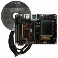
MCB2470
Manufacturer Part Number
MCB2470
Description
BOARD EVAL NXP LPC247X SERIES
Manufacturer
Keil
Type
MCUr
Specifications of MCB2470
Contents
Board, Cable, CD
For Use With/related Products
LPC2478
Lead Free Status / RoHS Status
Lead free / RoHS Compliant


NXP Semiconductors
Table 4.
LPC2478_1
Preliminary data sheet
Symbol
P2[8]/TD2/TXD2/
TRACEPKT3/
LCD[2]/LCD[6]
P2[9]/
USB_CONNECT1/
RXD2/EXTIN0/
LCD[3]/LCD[7]
P2[10]/EINT0
P2[11]/EINT1/
LCDCLKIN/
MCIDAT1/
I2STX_CLK
P2[12]/EINT2/
LCD[4]/LCD[3]/
LCD[8]/LCD[18]/
MCIDAT2/
I2STX_WS
P2[13]/EINT3/
LCD[5]/
LCD[9]/LCD[19]/
MCIDAT3/
I2STX_SDA
P2[14]/CS2/
CAP2[0]/SDA1
P2[15]/CS3/
CAP2[1]/SCL1
Pin description
Pin
134
132
110
108
106
102
91
99
[6]
[6]
[6]
[1]
[1]
[6]
[6]
[6]
…continued
Ball
H15
H16
N15
T17
N14
T16
R12
P13
[6]
[6]
[6]
[1]
[1]
[6]
[6]
[6]
Type
I/O
O
O
O
O
I/O
O
I
I
I
I/O
I
I/O
I
O
I/O
I/O
I/O
I
O
I/O
I/O
I/O
I
O
I/O
I/O
I/O
O
I
I/O
I/O
O
I
I/O
Rev. 01 — 9 February 2007
Description
P2[8] — General purpose digital input/output pin.
TD2 — CAN2 transmitter output.
TXD2 — Transmitter output for UART2.
TRACEPKT3 — Trace packet, bit 3.
LCD[2]/LCD[6] — LCD data.
P2[9] — General purpose digital input/output pin.
USB_CONNECT1 — USB1 SoftConnect control. Signal used to switch
an external 1.5 kΩ resistor under the software control. Used with the
SoftConnect USB feature.
RXD2 — Receiver input for UART2.
EXTIN0 — External Trigger Input.
LCD[3]/LCD[7] — LCD data.
P2[10] — General purpose digital input/output pin.
Note: LOW on this pin while RESET is LOW forces on-chip boot-loader
to take over control of the part after a reset.
EINT0 — External interrupt 0 input.
P2[11] — General purpose digital input/output pin.
EINT1 — External interrupt 1 input.
LCDCLKIN — LCD clock.
MCIDAT1 — Data line 1 for SD/MMC interface.
I2STX_CLK — Transmit Clock. It is driven by the master and received by
the slave. Corresponds to the signal SCK in the I
P2[12] — General purpose digital input/output pin.
EINT2 — External interrupt 2 input.
LCD[4]/LCD[3]/LCD[8]/LCD[18] — LCD data.
MCIDAT2 — Data line 2 for SD/MMC interface.
I2STX_WS — Transmit Word Select. It is driven by the master and
received by the slave. Corresponds to the signal WS in the I
specification.
P2[13] — General purpose digital input/output pin.
EINT3 — External interrupt 3 input.
LCD[5]/LCD[9]/LCD[19] — LCD data.
MCIDAT3 — Data line 3 for SD/MMC interface.
I2STX_SDA — Transmit data. It is driven by the transmitter and read by
the receiver. Corresponds to the signal SD in the I
P2[14] — General purpose digital input/output pin.
CS2 — LOW active Chip Select 2 signal.
CAP2[0] — Capture input for Timer 2, channel 0.
SDA1 — I
P2[15] — General purpose digital input/output pin.
CS3 — LOW active Chip Select 3 signal.
CAP2[1] — Capture input for Timer 2, channel 1.
SCL1 — I
2
2
C1 clock input/output (this is not an open-drain pin).
C1 data input/output (this is not an open-drain pin).
[18]
[17]
[17]
[17]
[18]
[18]
[18]
[17]
[18]
Fast communication chip
[18]
2
S-bus specification.
2
S-bus specification.
LPC2478
© NXP B.V. 2007. All rights reserved.
2
S-bus
18 of 76
Related parts for MCB2470
Image
Part Number
Description
Manufacturer
Datasheet
Request
R

Part Number:
Description:
KIT REF SYSTEM 78K0 UPD78F0712
Manufacturer:
Renesas Electronics America
Datasheet:
Part Number:
Description:
KIT DEMO EVAL 78K0R IE3
Manufacturer:
Renesas Electronics America
Datasheet:
Part Number:
Description:
KIT EVAL SYSTEM 78K0 UPD78F0714
Manufacturer:
Renesas Electronics America
Datasheet:

Part Number:
Description:
KEIL C-COMPILER INTERNATIONAL
Manufacturer:
Silicon Laboratories Inc
Part Number:
Description:
KEIL C-COMPILER US VERSION
Manufacturer:
Silicon Laboratories Inc

Part Number:
Description:
DEV KIT FOR STM32
Manufacturer:
STMicroelectronics
Datasheet:

Part Number:
Description:
KIT STARTER FOR STM32
Manufacturer:
STMicroelectronics
Datasheet:

Part Number:
Description:
KIT STARTER FOR STM32F10XE MCU
Manufacturer:
STMicroelectronics
Datasheet:

Part Number:
Description:
KIT STARTER KEIL FOR STR910
Manufacturer:
STMicroelectronics
Datasheet:


Part Number:
Description:
Microcontroller Modules & Accessories KEIL ULINK PRO 5V ADAPTOR KIT
Manufacturer:
Keil Software

Part Number:
Description:
BOARD EVAL FOR LPC213X ARM MCU
Manufacturer:
NXP Semiconductors
Datasheet:

Part Number:
Description:
K60N512 Keil Tower Kit
Manufacturer:
Freescale Semiconductor
Datasheet: