M53015EVB Freescale Semiconductor, M53015EVB Datasheet
M53015EVB
Specifications of M53015EVB


Related parts for M53015EVB

M53015EVB Summary of contents
Page 1
... Applicable Documents • MCF53017 Reference Manual • Universal Serial Bus Specification, Revision 2.0 © Freescale Semiconductor, Inc., 2010. All rights reserved. M53015EVBUM Rev. 0.5, 05/2010 Contents 1 Introduction . . . . . . . . . . . . . . . . . . . . . . . . . . . . . . . . . . . 1 2 Applicable Documents Evaluation Board Overview . . . . . . . . . . . . . . . . . . . . . . . 2 3 ...
Page 2
... Serial EEPROM • 32M x 16 Mobile DDR Power: • Inputs: — Input to the voltage regulator circuitry • Regulated On-board voltages: — 3 I/O Voltage — 1 Mobile DDR and Flash Voltage — 1 MCF53015 Core Voltage 2 M53015 Evaluation Board, Rev. 0.5 Freescale Semiconductor ...
Page 3
... EVB Block Diagram Freescale Semiconductor Figure 1. EVB Block Diagram M53015 Evaluation Board, Rev. 0.5 3 ...
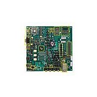
Page 4
... Board Diagram 4 Figure 2. Board Diagram M53015 Evaluation Board, Rev. 0.5 Freescale Semiconductor ...
Page 5
... GPIO, control structures or other I/Os. In Table 1, you'll find the details on how we've set up the first FlexBus region on the M53015EVB. We don't set up the second FlexBus memory region. Component Spansion 342-00474 ...
Page 6
... KB of MRAM are included on the M53015EVB. The MRAM is connected to CS1. The MRAM is a 3.3V part, so level translators are used to interface it to the 1.8V FlexBus. 5.6 Serial EEPROM The M53015EVB has a 256 KB serial EEPROM connected to the I2C bus that can be used for boot loader program storage. 6 Table 2. M53015EVB Clock Definitions ...
Page 7
... BDM and JTAG Interfaces — Processor The M53015EVB provides a BDM (Background Debug Mode) and JTAG Connector (26-pin header), J37, to give the end-user the ability to utilize the BDM/JTAG features of the MCF53015 processor. In addition, the M53015EVB provides an on board USB to BDM interface, J48. ...
Page 8
... Smart Card Interfaces The MCF53015 has two Smart Card interfaces, SIM0 and SIM1 pin SIM card socket is provided on the M53015EVB and connected to SIM0. The SIM_P0_VEN pin is accessible on TP5 and the pins of the SIM1 port are accessible through test points TP6 - TP10. ...
Page 9
... Ethernet The MCF53015 has 2 10/100 Ethernet MACs. On the M53015EVB these are each connected to National Semiconductor DP83640 ethernet PHYs. A dual port Ethernet jack, P2, is provided. Ethernet Channel 1 is connected to the upper port, while Channel 0 is connected to the lower port. Link, speed, and activity lights are provided for each port ...
Page 10
... I2C The I2C bus of the MCF53015 is used in several places on the M53015EVB connected to a serial EEPROM, a USB OTG Charge Pump, and a programmable clock generator. These pins are also accessible on the University Breakout Connector, J1. Table 3 below defines the device addresses for the devices connected to the I2C bus ...
Page 11
... A19 ON OFF SW3-1 A20 ON OFF Freescale Semiconductor Table 10. SW3, SW4, and SW5 Settings 1 Boot from FlexBus with defaults, unified SDR bus/FlexBus Boot from FlexBus with defaults, split DDR bus/FlexBus Boot from FlexBus and override defaults via address bus (FB_A[21:17]) Reserved Master Mode ...
Page 12
... Bold indicates the default setting, SW4-3, SW4-4, and SW3-4 are not connected and their position does not affect configuration. 5.23 Jumpers, Headers, and Switches Headers and jumpers on the M53015EVB allow for user control of the hardware configuration. The following tables provide descriptions for each of these settings: 1,2 Reference Designator Setting ...
Page 13
... Connects the DSPI_PCS3/USB1_VBUS_EN line to the Enable B pin of the USB power ON distribution chip (for USB OTG operation) H27 Disconnects the DSPI_PCS3/USB1_VBUS_EN line from the Enable B pin of the USB OFF power distribution chip (for DSPI operation) Freescale Semiconductor Table 11. Header Settings (continued) Function M53015 Evaluation Board, Rev. 0.5 13 ...
Page 14
... Type A socket, J50 Connects a 15K pulldown resistor to the D+ line of the USB Host connected to the Type A socket, J50 Disconnects the 15K pulldown resistor from the D+ line of the USB Host connected to the Type A socket, J50 M53015 Evaluation Board, Rev. 0.5 Function Freescale Semiconductor ...
Page 15
... Connects the Mic In line to the Microphone In jack, J25 1-2 Connects the Mic Bias line to the On-board microphone, P4 J22 2-3 Connects the Mic Bias line to the bias circuit of the Microphone In jack, J25 Freescale Semiconductor Table 12. Jumper Settings Function M53015 Evaluation Board, Rev. 0.5 15 ...
Page 16
... Selects the SMA connector, J47 as an external clock source for XTAL_32K, depending on 1-2 the setting of J43 J42 2-3 Selects the on-board 32.768KHz oscillator as the clock source for XTAL_32K, depending on the setting of J43 16 Table 12. Jumper Settings Function M53015 Evaluation Board, Rev. 0.5 Freescale Semiconductor ...
Page 17
... Bold indicates the default setting 2 ON indicates that a shunt should be fitted on the jumper; OFF indicates that no shunt should be applied. Freescale Semiconductor Table 12. Jumper Settings Selects the Oscillator/External option as the external clock source for XTAL_32K Selects the on-board 32.768KHz crystal as the clock source between XTAL_32K and ...
Page 18
... J50 USB Host Type A Socket J51 Barrel type Power Jack, 5V center positive, 1.93mm center pin diameter J52 DB9 Socket, connected to UART1 or UART2 depending on jumper settings J53 USB Mini A/B connector for USB OTG P4 Microphone M53015 Evaluation Board, Rev. 0.5 Freescale Semiconductor ...
Page 19
... The following table provides a description of the various switches on the board. Reference Designator Freescale Semiconductor Table 14. Switches Function SW1 Abort Reset push button - Connected to IRQ7_B SW2 Board Reset push button SW3 Board Configuration switch. See Boot Options section for more information. SW4 Board Configuration switch ...
Page 20
... GND CS_B0 FB_CLK TS_B SIM_P0_VEN SIM_P1_RST SIM_P1_SCLK SIM_P1_XMT SIM_P1_PD SIM_P1_VEN HP_OUT RW_B GND OE_B RDY RESET_B SD_SDR_DQS RSTOUT_B TA_B CLKB1 (From Zero Delay Clock Buffer, U12) CLKB (From Programmable Clock Generator, U14) GND GND M53015 Evaluation Board, Rev. 0.5 Freescale Semiconductor ...