DK-DEV-2AGX125N Altera, DK-DEV-2AGX125N Datasheet
DK-DEV-2AGX125N
Specifications of DK-DEV-2AGX125N
Available stocks


Related parts for DK-DEV-2AGX125N


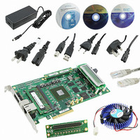
DK-DEV-2AGX125N Summary of contents
Page 1
... Arria II GX FPGA Development Board Reference Manual 101 Innovation Drive San Jose, CA 95134 www.altera.com MNL-01047-1.2 Arria II GX FPGA Development Board Reference Manual Subscribe ...
Page 2
... Altera warrants performance of its semiconductor products to current specifications in accordance with Altera’s standard warranty, but reserves the right to make changes to any products and services at any time without notice. Altera assumes no responsibility or liability arising out of the application or use of any information, product, or service described herein except as expressly agreed to in writing by Altera. Altera customers are advised to obtain the latest version of device specifications before relying on any published information and before placing orders for products or services ...
Page 3
... High-Speed Mezzanine Cards . . . . . . . . . . . . . . . . . . . . . . . . . . . . . . . . . . . . . . . . . . . . . . . . . . . . . . . . . 2–32 Memory . . . . . . . . . . . . . . . . . . . . . . . . . . . . . . . . . . . . . . . . . . . . . . . . . . . . . . . . . . . . . . . . . . . . . . . . . . . . . . . 2–39 DDR3 . . . . . . . . . . . . . . . . . . . . . . . . . . . . . . . . . . . . . . . . . . . . . . . . . . . . . . . . . . . . . . . . . . . . . . . . . . . . . . 2–39 DDR2 SODIMM . . . . . . . . . . . . . . . . . . . . . . . . . . . . . . . . . . . . . . . . . . . . . . . . . . . . . . . . . . . . . . . . . . . . . 2–41 SSRAM . . . . . . . . . . . . . . . . . . . . . . . . . . . . . . . . . . . . . . . . . . . . . . . . . . . . . . . . . . . . . . . . . . . . . . . . . . . . . 2–45 Flash . . . . . . . . . . . . . . . . . . . . . . . . . . . . . . . . . . . . . . . . . . . . . . . . . . . . . . . . . . . . . . . . . . . . . . . . . . . . . . . 2–48 Power Supply . . . . . . . . . . . . . . . . . . . . . . . . . . . . . . . . . . . . . . . . . . . . . . . . . . . . . . . . . . . . . . . . . . . . . . . . . . 2–49 Power Distribution System . . . . . . . . . . . . . . . . . . . . . . . . . . . . . . . . . . . . . . . . . . . . . . . . . . . . . . . . . . . . 2–50 Power Measurement . . . . . . . . . . . . . . . . . . . . . . . . . . . . . . . . . . . . . . . . . . . . . . . . . . . . . . . . . . . . . . . . . 2–51 Statement of China-RoHS Compliance . . . . . . . . . . . . . . . . . . . . . . . . . . . . . . . . . . . . . . . . . . . . . . . . . . . . 2–52 February 2011 Altera Corporation Contents Arria II GX FPGA Development Board Reference Manual ...
Page 4
... Appendix A. Board Revision History Single-Die Flash Version Differences . . . . . . . . . . . . . . . . . . . . . . . . . . . . . . . . . . . . . . . . . . . . . . . . . . . . . . A–1 Additional Information Document Revision History . . . . . . . . . . . . . . . . . . . . . . . . . . . . . . . . . . . . . . . . . . . . . . . . . . . . . . . . . . . Info–1 How to Contact Altera . . . . . . . . . . . . . . . . . . . . . . . . . . . . . . . . . . . . . . . . . . . . . . . . . . . . . . . . . . . . . . . . Info–1 Typographic Conventions . . . . . . . . . . . . . . . . . . . . . . . . . . . . . . . . . . . . . . . . . . . . . . . . . . . . . . . . . . . . . Info–2 Arria II GX FPGA Development Board Reference Manual ContentsContents February 2011 Altera Corporation ...
Page 5
... The board provides a wide range of peripherals and memory interfaces to facilitate the development of the Arria II GX FPGA designs. Two high-speed mezzanine card (HSMC) ports are available to add additional functionality via a variety of HSMCs available from Altera f To see a list of the latest HSMCs available or to download a copy of the HSMC specification, refer to the website ...
Page 6
... Programmable oscillator with a default frequency of 100-MHz ■ SMA connectors for external LVPECL clock input ■ SMA connector for clock output ■ Arria II GX FPGA Development Board Reference Manual TM ® for use with the Quartus II Programmer February 2011 Altera Corporation Chapter 1: Overview Board Component Blocks ...
Page 7
... PCI Express edge connector power ■ On-board power measurement circuitry ■ ■ Mechanical PCI Express full-length standard-height (8.48” x 4.376”) ■ PCI Express chassis or bench-top operation ■ February 2011 Altera Corporation Arria II GX FPGA Development Board Reference Manual 1–3 ...
Page 8
... EP2AGX125EF35 CPLD x8 Edge Chapter 1: Overview Development Board Block Diagram Z Z USB Embedded 2.0 Blaster JTAG Chain x50 128 Mbyte DDR3 (x16) x11 2x16 LCD x3 Push-button Switches x4 DIP Switch x4 LEDs x26 ADDR x32 DATA 64 Mbyte 2 Mbyte Flash SSRAM February 2011 Altera Corporation ...
Page 9
... Supply” on page 2–49 ■ ■ “Statement of China-RoHS Compliance” on page 2–52 February 2011 Altera Corporation 2. Board Components illustrates major component locations and Arria II GX FPGA Development Kit User Arria II GX FPGA Development Board Reference Manual Table 2–1 provides a brief Guide ...
Page 10
... Configuration LEDs (D11-D16) Load Image (PB5), Image Select Push-button Switch (PB6) DDR3 x16 (U13) Power Switch (SW1) DC Input Jack (J4) SSRAM x36 Memory (U22) Character LCD (J3) Flash x16 Memory (U23) Fan Power (J13) Board Settings DIP Switch (SW4) Description February 2011 Altera Corporation ...
Page 11
... General user push-button PB1, PB2 switches Image select push-button PB6 switch February 2011 Altera Corporation Description Illuminates when the MAX II CPLD EPM2210 System Controller is actively configuring the FPGA. Illuminates when the FPGA configuration from flash memory fails. Illuminates when 2.5-V power is present. ...
Page 12
... USB interface for programming the FPGA through embedded USB-Blaster JTAG via a type-B USB cable. RJ-45 connector which provides a 10/100/1000 Ethernet connection via a Marvell 88E1111 PHY and the FPGA-based Altera Triple Speed Ethernet MegaCore function in RGMII mode. Connector which interfaces to the 16 character × 2 line LCD module along with two standoffs at MTH7 and MTH8 ...
Page 13
... I/O Resources Figure 2–2 illustrates the bank organization and I/O count for the EP2AGX125 and EP2AGX260 device in the 1152-pin FBGA package. Figure 2–2. EP2AGX125 and EP2AGX260 Device I/O Bank Diagram February 2011 Altera Corporation Total RAM 18-bit × 18-bit PLLs Kbits ...
Page 14
... Special Pins 2 Diff ×8 DQS 8 Diff ×8 DQS — — 1 REFCLK, 8 XCVR 4 XCVR, 17 LVDS, 5 Clock Inputs 4 XCVR, 1 Clock Input 1 Clock Input 1 DEV_CLRn — — — 5 REFCLK PLLs Transceivers Package Type 6 16 1152-pin FBGA February 2011 Altera Corporation (1) ...
Page 15
... User Input/Output” on page available in the Arria II GX EP2AGX260EF35 device to support an extra transceiver quadrant and additional I/O banks. MAX II CPLD EPM2210 System Controller The board utilizes the EPM2210 System Controller, an Altera MAX II CPLD, for the following purposes: FPGA configuration from flash memory ■ ...
Page 16
... FSM bus flash memory chip enable C9 N4 FSM bus flash memory clock E7 K5 FSM bus flash memory output enable D8 R3 FSM bus flash memory ready D15 N3 FSM bus flash memory reset Chapter 2: Board Components MAX II CPLD EPM2210 System Controller Description February 2011 Altera Corporation ...
Page 17
... February 2011 Altera Corporation EPM2210 EP2AGX125 Pin Number Pin Number D7 C7 FSM bus flash memory write enable J1 AE25 FPGA configuration done B1 N26 FPGA configuration data A4 N6 ...
Page 18
... Flash memory image select indicator A8 — Flash memory image select indicator B7 — Flash memory image select indicator B9 — Toggles the LED_CONFIG_LED[2:0] sequence. K13 — DIP - MAX II LCD drive enable Chapter 2: Board Components MAX II CPLD EPM2210 System Controller Description February 2011 Altera Corporation ...
Page 19
... Table 2–8. MAX II CPLD EPM2210 System Controller Component Reference and Manufacturing Information Board Reference Description IC - MAX II CPLD EPM2210 U32 256FBGA -3 LF 2.5V VCCINT February 2011 Altera Corporation EPM2210 EP2AGX125 Pin Number Pin Number Load the flash memory identified by the A9 — ...
Page 20
... FPGA Programming over Embedded USB-Blaster The board implements a USB-Blaster using a USB Type-B connector (J6), a FTDI USB 2.0 PHY device (U15), and an Altera MAX IIZ CPLD (U10). This allows the configuration of the FPGA using a USB cable directly connected between the USB port on the board (J6) and a USB port running the Quartus II software ...
Page 21
... The MAX II CPLD EPM2210 System Controller must be in the chain to use some of the GUI interfaces. For this setting, remove the left-most jumper shunt from the JTAG chain header (J9). Flash Memory Programming Flash memory programming is possible through a variety of methods using the Arria II GX device. February 2011 Altera Corporation 10-pin J5 JTAG Connector TCK GPIO ...
Page 22
... The development board implements the Altera PFL megafunction for flash memory programming. The PFL megafunction is a block of logic that is programmed into an Altera programmable logic device (FPGA or CPLD). The PFL functions as a utility for writing to a compatible flash memory device. This ...
Page 23
... FLASH_CEn FLASH_OEn FLASH_WEn FLASH_ADVn FLASH_CLK FLASH_RSTn FLASH_RSTn FLASH_RYBSYn Table 2–9 shows the flash memory map storage. Table 2–9. Flash Memory Map (Part Unused February 2011 Altera Corporation 2.5 V 2.5 V 100 Ω 10 kΩ 100 MHz CONF_DONE_LED 2 kΩ Name Size (KB) 32 ...
Page 24
... Configuration, Status, and Setup Elements Address 0x03FD-FFFF 0x0282-0000 0x0281-FFFF 0x0202-0000 0x0201-FFFF 0x0182-0000 0x0181-FFFF 0x0128-0000 0x0127-FFFF 0x00C6-0000 0x00C5-FFFF 0x0064-0000 0x0063-FFFF 0x0002-0000 0x0001-FFFF 0x0001-8000 0x0001-7FFF 0x0001-0000 0x0000-FFFF 0x0000-8000 0x0000-7FFF 0x0000-0000 Table 2–10 defines the hardware (1) (2) Design Factory hardware User hardware 1 User hardware 2 February 2011 Altera Corporation ...
Page 25
... Present HSMC Port B D1 Present D24 PCIe x1 February 2011 Altera Corporation Arria II GX FPGA Development Kit User Arria II GX FPGA Development Kit User Parallel Flash Loader Megafunction User Description Blue LED. Illuminates when 2.5 V power is active. Green LED. Illuminates when the FPGA is successfully configured. Driven by the MAX II CPLD EPM2210 System Controller ...
Page 26
... Green LED. Configure this LED to display the PCI Express link width x8. Manufacturer Manufacturer Part Number Lite-On LTST-C170KGKT Lite-On LTST-C170KRKT Lite-On LTST-C170TBKT Description Chapter 2: Board Components Configuration, Status, and Setup Elements Manufacturer Website www.us.liteon.com/opto.index.html www.us.liteon.com/opto.index.html www.us.liteon.com/opto.index.html Table 2–13 shows the Default OFF OFF OFF OFF OFF OFF February 2011 Altera Corporation ...
Page 27
... JTAG chain header component reference and manufacturing information. Table 2–16. JTAG Chain Header Component Reference and Manufacturing Information Board Reference Device Description J9 2x4 100 mil jumper February 2011 Altera Corporation Description Manufacturer Manufacturer Part Number HCH HPS608-E Table 2–15 ...
Page 28
... Not used Manufacturer HCH HPS604-E Table 2–10 Manufacturer Manufacturer Part Number Dawning Precision Co. TS-A02SA-2-S100 Chapter 2: Board Components Configuration, Status, and Setup Elements Default OFF Manufacturer Manufacturer Website Part Number www.hchtwn.com.tw for the LED_CONFIG_LED[2:0] Manufacturer Website http://www.dawning2.com.tw/ company.php February 2011 Altera Corporation ...
Page 29
... MHz Crystal Table 2–20 shows the external clock inputs for the Arria II GX FPGA development board. Table 2–20. Arria II GX FPGA Development Board Clock Inputs (Part Source Schematic Signal Name CLK_155_P U25 CLK_155_N February 2011 Altera Corporation ENET_RX_CLK (LVDS) (2 PLL PLL ...
Page 30
... Can also support two LVTTL J18 inputs. Single-ended input from the installed HSMC AP16 LVTTL port B cable or board. AE29 High-Speed Current Steering Logic (HCSL) HCSL input from the PCI Express edge connector. AE30 Chapter 2: Board Components Clock Circuitry Description February 2011 Altera Corporation ...
Page 31
... Table 2–21. Arria II GX FPGA Development Board Clock Outputs Connector Schematic Signal Name SMA CLKOUT_SMA Samtec HSMC HSMA_CLKOUT0 HSMA_CLKOUT_P1 Samtec HSMC HSMA_CLKOUT_N1 HSMA_CLKOUT_P2 Samtec HSMC HSMA_CLKOUT_N2 Samtec HSMC HSMB_CLKOUT0 February 2011 Altera Corporation HSMA_CLKOUT_P[2]/N[2] (LVDS) (LVDS PLL PLL PLL 2 PLL ...
Page 32
... Epson 50.0000M-DCL3 “Reset Configuration Push- 2–20. Schematic Signal I/O Standard Name USER_PB0 USER_PB1 CPU_RESET Chapter 2: Board Components General User Input/Output Manufacturer Website www.eea.epson.com www.ti.com www.ti.com www.mecxtal.com www.eea.epson.com Arria II GX Device Pin Number AK9 1.8-V AL7 2.5-V N10 February 2011 Altera Corporation ...
Page 33
... LEDs from the FPGA designs loaded into the Arria II GX device. The LEDs illuminate when a logic 0 is driven, and turns off when a logic 1 is driven. There is no board-specific function for these LEDs. February 2011 Altera Corporation Manufacturer Manufacturer Part Number Dawning Precision Co ...
Page 34
... Part Number Lite-On LTST-C170KGKT Schematic I/O Standard Signal Name HSMA_TX_LED HSMA_RX_LED HSMB_TX_LED HSMB_RX_LED Chapter 2: Board Components General User Input/Output Arria II GX Device Pin Number G1 J4 2.5 Manufacturer Website www.us.liteon.com/opto.index.html Arria II GX Device Pin Number C29 N5 2.5-V AE24 AE23 February 2011 Altera Corporation ...
Page 35
... LCD pin definitions, and is an excerpt from the Lumex data sheet. Table 2–32. LCD Pin Definitions and Functions (Part Pin Number February 2011 Altera Corporation Manufacturer Manufacturer Part Number Lite-On LTST-C170KGKT Schematic Signal Name LCD_DATA0 LCD_DATA1 LCD_DATA2 LCD_DATA3 LCD_DATA4 ...
Page 36
... H/L L: Data write (MPU to module Enable H/L Data bus, software selectable 4-bit or 8-bit mode Manufacturer Samtec TSM-107-01-G-DV Lumex Inc. LCM-S01602DSR/C Guide. Chapter 2: Board Components Components and Interfaces Function Manufacturer Manufacturer Part Number Website www.samtec.com www.lumex.com PCI Express February 2011 Altera Corporation ...
Page 37
... J14.B24 Add-in card receive bus J14.B27 Add-in card receive bus J14.B28 Add-in card receive bus J14.B33 Add-in card receive bus J14.B34 Add-in card receive bus February 2011 Altera Corporation = 1.15 V REFCLK – = 550 mV = 250 mV REFCLK + = –0.30 V MIN Schematic Signal Name PCIE_RX_P0 ...
Page 38
... PCIE_TX_N5 PCIE_TX_P6 PCIE_TX_N6 PCIE_TX_P7 PCIE_TX_N7 PCIE_REFCLK_P HCSL PCIE_REFCLK_N PCIE_PERSTn PCIE_WAKEn PCIE_SMBCLK LVTTL PCIE_SMBDAT PCIE_LED_X1 PCIE_LED_X4 PCIE_LED_X8 February 2011 Altera Corporation Components and Interfaces Arria II GX Device Pin Number AC33 AC34 AA33 AA34 W33 W34 AM31 AM32 AK31 AK32 AH31 AH32 AF31 ...
Page 39
... U24.94 RGMII receive control U24.11 RGMII transmit data U24.12 RGMII transmit data U24.14 RGMII transmit data U24.16 RGMII transmit data U24.9 RGMII transmit control February 2011 Altera Corporation Marvell 88E1111 Transformer PHY Device Schematic Signal Name ENET_GTX_CLK ENET_INTn ENET_MDC ENET_MDIO ENET_RESETn ...
Page 40
... The HSMC interface also allows JTAG, SMB, clock outputs and inputs, as well as power for compatible HSMC cards. The HSMC is an Altera-developed open specification, which allows you to expand the functionality of the development board through the addition of daughtercards (HSMCs). ...
Page 41
... Dedicated CMOS clock in J2.41 Dedicated CMOS I/O bit 0 J2.42 Dedicated CMOS I/O bit 1 J2.43 Dedicated CMOS I/O bit 2 J2.44 Dedicated CMOS I/O bit 3 February 2011 Altera Corporation High Speed Mezzanine Card (HSMC) Specification Schematic Signal Name HSMA_TX_P3 HSMA_RX_P3 HSMA_TX_N3 HSMA_RX_N3 HSMA_TX_P2 ...
Page 42
... HSMA_TX_D_P5 HSMA_RX_D_P5 HSMA_TX_D_N5 HSMA_RX_D_N5 HSMA_TX_D_P6 HSMA_RX_D_P6 HSMA_TX_D_N6 HSMA_RX_D_N6 HSMA_TX_D_P7 HSMA_RX_D_P7 HSMA_TX_D_N7 HSMA_RX_D_N7 HSMA_CLKOUT_P1 HSMA_CLKIN_P1 HSMA_CLKOUT_N1 HSMA_CLKIN_N1 HSMA_TX_D_P8 HSMA_RX_D_P8 February 2011 Altera Corporation Arria II GX Device Pin Number AA10 AC5 AA9 AC4 Y11 AE4 Y10 AF4 AH2 AF1 AH1 AG1 AB10 AE2 ...
Page 43
... J2.155 LVDS or CMOS clock out 2 or CMOS bit 76 J2.156 LVDS or CMOS clock CMOS bit 77 J2.157 LVDS or CMOS clock out 2 or CMOS bit 78 J2.158 LVDS or CMOS clock CMOS bit 79 February 2011 Altera Corporation Schematic Signal I/O Standard Name HSMA_TX_D_N8 HSMA_RX_D_N8 HSMA_TX_D_P9 HSMA_RX_D_P9 ...
Page 44
... HSMB_RX_N1 HSMB_TX_P0 HSMB_RX_P0 HSMB_TX_N0 HSMB_RX_N0 HSMB_SDA HSMB_SCL JTAG_TCK JTAG_TMS JTAG_HSMB_TDO 2.5-V JTAG_HSMB_TDI HSMB_CLKOUT0 HSMB_CLKIN0 HSMB_D0 HSMB_D1 HSMB_D2 February 2011 Altera Corporation Arria II GX Device Pin Number U3 N5 C29 Arria II GX Device Pin Number B31 C33 B32 C34 D31 E33 D32 E34 ...
Page 45
... J1.95 Dedicated CMOS I/O bit 36 J1.96 Dedicated CMOS I/O bit 37 J1.97 Dedicated CMOS I/O bit 38 J1.98 Dedicated CMOS I/O bit 39 J1.101 Dedicated CMOS I/O bit 40 February 2011 Altera Corporation Schematic Signal I/O Standard Name HSMB_D3 HSMB_D4 HSMB_D5 HSMB_D6 HSMB_D7 2.5-V HSMB_D8 ...
Page 46
... HSMB_D62 HSMB_D63 HSMB_D64 2.5-V HSMB_D65 HSMB_D66 HSMB_D67 HSMB_D68 HSMB_D69 HSMB_D70 HSMB_D71 HSMB_D72 HSMB_D73 — — HSMB_CLKOUT_P2 HSMB_D74 HSMB_CLKOUT_N2 February 2011 Altera Corporation Arria II GX Device Pin Number AL2 AK3 AL1 AJ4 AK1 AJ3 AJ1 AJ2 AH3 AH6 AH4 AC10 M10 AC11 ...
Page 47
... MHz for a maximum theoretical bandwidth of over 12.8 Gbps. The internal bus in the FPGA is typically times the width at full-rate or half-rate respectively. For example, a 400 MHz 16-bit interface becomes a 200 MHz 64-bit bus. February 2011 Altera Corporation Schematic Signal Name HSMB_D75 ...
Page 48
... SSTL Class I DDR3_A12 DDR3_A13 DDR3_A14 DDR3_BA0 DDR3_BA1 DDR3_BA2 DDR3_CAS_n DDR3_CKE DDR3_CS_n DDR3_ODT DDR3_RAS_n DDR3_RST_n DDR3_WE_n DDR3_CLK_P Differential 1.5-V SSTL Class I DDR3_CLK_N February 2011 Altera Corporation Memory Arria II GX Device Pin Number G16 A12 H18 F16 A7 G17 C13 K14 D11 M16 A11 E15 A8 ...
Page 49
... This memory interface runs at a maximum fequency of 333 MHz for a maximum theoretical bandwidth of over 42.6 Gbps. The internal bus in the FPGA is typically times the width at full rate or half rate respectively. For example, a 333 MHz 64-bit interface becomes a 166.5 MHz 256-bit bus. February 2011 Altera Corporation Schematic Signal I/O Standard Name ...
Page 50
... DDR2_BA2 DDR2_CAS_n DDR2_CKE0 DDR2_CS_n0 DDR2_CS_n1 DDR2_ODT0 DDR2_ODT1 DDR2_RAS_n DDR2_SCL DDR2_SDA DDR2_WE_n DDR2_CLK_P0 DDR2_CLK_N0 Differential 1.8-V SSTL Class I DDR2_CLK_P1 DDR2_CLK_N1 February 2011 Altera Corporation Memory Arria II GX Device Pin Number AH14 AK12 AE12 AH13 AF14 AG12 AJ18 AL19 AG13 AE13 AK10 AH23 ...
Page 51
... J7.61 Data bus byte lane 3 J7.63 Data bus byte lane 3 J7.73 Data bus byte lane 3 J7.75 Data bus byte lane 3 J7.62 Data bus byte lane 3 February 2011 Altera Corporation Schematic Signal I/O Standard Name DDR2_DQ0 DDR2_DQ1 DDR2_DQ2 DDR2_DQ3 DDR2_DQ4 DDR2_DQ5 DDR2_DQ6 ...
Page 52
... DDR2_DQ43 DDR2_DQ44 DDR2_DQ45 DDR2_DQ46 DDR2_DQ47 DDR2_DM5 DDR2_DQS5 DDR2_DQSN5 DDR2_DQ48 DDR2_DQ49 DDR2_DQ50 DDR2_DQ51 DDR2_DQ52 DDR2_DQ53 DDR2_DQ54 DDR2_DQ55 DDR2_DM6 DDR2_DQS6 February 2011 Altera Corporation Memory Arria II GX Device Pin Number AN19 AK18 AF18 AP20 AL18 AM18 AP15 AN15 AH17 AF17 AC18 AE17 AP14 ...
Page 53
... Table 2–44. SSRAM Pin Assignments, Schematic Signal Names, and Functions (Part Board Reference Description U22.R6 Address bus U22.P6 Address bus U22.A2 Address bus February 2011 Altera Corporation Schematic Signal I/O Standard Name DDR2_DQSN6 DDR2_DQ56 DDR2_DQ57 DDR2_DQ58 DDR2_DQ59 DDR2_DQ60 1.8-V SSTL Class I ...
Page 54
... Pin Number C8 N9 D20 A23 B24 C24 E25 F21 J19 H19 K21 L21 F25 F26 G23 H21 M13 P7 A19 C18 D28 B19 E19 E18 G19 F19 D21 D23 D24 A25 B25 A26 C26 A27 R9 R10 R8 A17 D22 February 2011 Altera Corporation ...
Page 55
... SSRAM component reference and manufacturing information. Table 2–45. SSRAM Component Reference and Manufacturing Information Board Reference Description Standard synchronous pipelined U22 SCD, 512K × 36, 200 MHz February 2011 Altera Corporation I/O Standard Schematic Signal Name FSM_D21 FSM_D22 FSM_D23 FSM_D24 ...
Page 56
... FSM_A11 FSM_A12 FSM_A13 2.5-V FSM_A14 FSM_A15 FSM_A16 FSM_A17 FSM_A18 FSM_A19 FSM_A20 FSM_A21 FSM_A22 FSM_A23 FSM_A24 FSM_A25 FSM_D0 February 2011 Altera Corporation Chapter 2: Board Components Memory Arria II GX Device Pin Number J3 D29 J21 L13 C8 N9 D20 A23 B24 C24 E25 F21 J19 ...
Page 57
... HSMC connectors. An on-board multi-channel analog-to-digital converter (ADC) measures both the voltage and current for several specific board rails. A GUI displays the power utilization by showing a graph of the power consumption versus time. February 2011 Altera Corporation I/O Standard Schematic Signal Name FSM_D1 FSM_D2 ...
Page 58
... SENSE A2VCCD PLL 0.9 V 0.071 A A2GX Digital PLL R SENSE 5.0V_MONITOR 5 LT2418 0.010 A 3.3V 3.3 V HSMC Port A and B 4.100 A 2 LVDS Clock Buffer R A2VCCA SENSE 2.5 V 0.091 A A2GX GXB PMA R SENSE A2VCCA PLL 2.5 V 0.052 A A2GX Analog PLL February 2011 Altera Corporation ...
Page 59
... Table 2–48. Power Rails Measurement Based on the Rotary Switch Position (Part Switch Schematic Signal Name 0 A2VCCIO_B3B_B5B_B6B 1 A2VCCIO_B5A 2 A2VCCIO_B6A 3 A2VCCIO_B7B_B8A 4 A2VCCPD A2VCCIO_B3A_B4 5 6 A2VCCIO_B7A 7 A2VCCH_GXB February 2011 Altera Corporation Embedded USB-Blaster EPM 240 Z Power Supply Load #0 JTAG Chain EPM2210 Power Supply Load #13 U16 SCK DSI 8 Ch. DSO CSn LTC2418 U11 SCK DSI 8 Ch ...
Page 60
... PLL analog power 2.5 VCCA XCVR PMA regulator Manufacturing Manufacturer Part Number Linear Technology LTC2418CGN#PBF Notes (1), Hexavalent Cadmium Mercury Chromium (Cd) (Hg) (Cr6 Chapter 2: Board Components Statement of China-RoHS Compliance Description Manufacturer Website www.linear.com (2) Polybrominated Polybrominated diphenyl Ethers biphenyls (PBB) (PBDE February 2011 Altera Corporation ...
Page 61
... U23. The single-die package is smaller than the dual-die version. f For more information about the flash change and its application, refer to the GX FPGA Development Kit User February 2011 Altera Corporation A. Board Revision History Description Increased the maximum speeds of the following interfaces: LVDS incresases to 1.25 Mbps from 1.05 Mbps. ■ ...
Page 62
... A–2 Arria II GX FPGA Development Board Reference Manual Appendix A: Board Revision History Single-Die Flash Version Differences February 2011 Altera Corporation ...
Page 63
... Contact Technical support Technical training Product literature Non-technical support (General) (Software Licensing) Note to Table: (1) You can also contact your local Altera sales office or sales representative. February 2011 Altera Corporation Changes “DDR3” and “DDR2 SODIMM” sections to reflect the interface modification in Table 2– ...
Page 64
... A warning calls attention to a condition or possible situation that can cause you injury. The envelope links to the Email Subscription Management Center website, where you can sign up to receive update notifications for Altera documents. Additional InformationAdditional Information Typographic Conventions page of the Altera February 2011 Altera Corporation ...