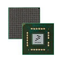
MPC8536DS Freescale Semiconductor, MPC8536DS Datasheet - Page 108

MPC8536DS
Manufacturer Part Number
MPC8536DS
Description
BOARD DEV SYSTEM MPC8536E
Manufacturer
Freescale Semiconductor
Series
PowerQUICC III™r
Type
MPUr
Datasheets
1.MPC8536EBVTAVLA.pdf
(127 pages)
2.MPC8536EBVTAVLA.pdf
(1706 pages)
3.MPC8536DS.pdf
(2 pages)
4.MPC8536DS.pdf
(126 pages)
Specifications of MPC8536DS
Contents
Board, Software and Documentation
Processor Series
MPC85xx
Core
e500
Data Bus Width
32 bit
Maximum Clock Frequency
667 MHz
Operating Supply Voltage
- 0.3 V to + 1.21 V
Maximum Operating Temperature
+ 105 C
Data Ram Size
32 KB
Interface Type
SPI, USB
Program Memory Type
DDR2, DDR3, SDRAM
Core Size
32 Bit
Program Memory Size
544KB
Cpu Speed
1.5GHz
Digital Ic Case Style
BGA
No. Of Pins
783
Supply Voltage Range
0.95V To 1.05V
Rohs Compliant
Yes
For Use With/related Products
MPC8536
Lead Free Status / RoHS Status
Lead free / RoHS Compliant
Clocking
2.23.2
The CCB clock is the clock that drives the e500 core complex bus (CCB), and is also called the platform clock. The frequency
of the CCB is set using the following reset signals, as shown in
Note that there is no default for this PLL ratio; these signals must be pulled to the desired values.
2.23.3
Table 76
by the binary value of LBCTL, LALE and LGPL2 at power up, as shown in
2.23.4
The DDR memory controller complex can be synchronous with, or asynchronous to, the CCB, depending on configuration.
Table 77
DDRCLK, which is not the memory bus clock.
When synchronous mode is selected, the memory buses are clocked at half the CCB clock rate. The default mode of operation
is for the DDR data rate for the DDR controller to be equal to the CCB clock rate in synchronous mode, or the resulting DDR
PLL rate in asynchronous mode.
In asynchronous mode, the DDR PLL rate to DDRCLK ratios listed in
since the DDR PLL rate in asynchronous mode means the DDR data rate resulting from DDR PLL output.
108
•
•
SYSCLK input signal
Binary value on LA[28:31] at power up
describes the clock ratio between the e500 core complex bus (CCB) and the e500 core clock. This ratio is determined
describes the clock ratio between the DDR memory controller complex and the DDR/DDRCLK PLL reference clock,
Binary Value of
LGPL2 Signals
LBCTL, LALE,
CCB/SYSCLK PLL Ratio
e500 Core PLL Ratio
DDR/DDRCLK PLL Ratio
000
001
010
011
LA[28:31] Signals
Binary Value of
MPC8536E PowerQUICC III Integrated Processor Hardware Specifications, Rev. 3
0000
0001
0010
0011
0100
0101
0110
0111
e500 core: CCB Clock Ratio
Table 76. e500 Core to CCB Clock Ratio
CCB:SYSCLK Ratio
Reserved
4:1
9:2
3:2
Reserved
Reserved
Reserved
Table 75. CCB Clock Ratio
16:1
3:1
4:1
5:1
6:1
Table
LA[28:31] Signals
Binary Value of
LGPL2 Signals
Binary Value of
LBCTL, LALE,
75:
1000
1001
1010
1011
1100
1101
1110
1111
Table 77
100
101
110
111
Table
reflects the DDR data rate to DDRCLK ratio,
76.
e500 core: CCB Clock Ratio
CCB:SYSCLK Ratio
Reserved
Reserved
Reserved
Reserved
10:1
12:1
8:1
9:1
2:1
5:2
3:1
7:2
Freescale Semiconductor


