C8051F206DK Silicon Laboratories Inc, C8051F206DK Datasheet - Page 128
C8051F206DK
Manufacturer Part Number
C8051F206DK
Description
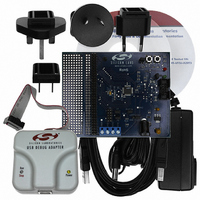
DEV KIT FOR C8051F206
Manufacturer
Silicon Laboratories Inc
Type
MCUr
Specifications of C8051F206DK
Contents
Evaluation Board, Power Supply, USB Cables, Adapter and Documentation
Processor To Be Evaluated
C8051F206
Interface Type
USB
Lead Free Status / RoHS Status
Contains lead / RoHS non-compliant
For Use With/related Products
Silicon Laboratories C8051F206
Lead Free Status / Rohs Status
Lead free / RoHS Compliant
Other names
336-1237


C8051F2xx
17.1.4. Mode 3: Two 8-bit Counter/Timers (Timer 0 Only)
Timer 0 and Timer 1 behave differently in Mode 3. Timer 0 is configured as two separate 8-bit counter/tim-
ers held in TL0 and TH0. The counter/timer in TL0 is controlled using the Timer 0 control/status bits in
TCON and TMOD: TR0, C/T0, GATE0 and TF0. It can use either the system clock or an external input sig-
nal as its time base. The TH0 register is restricted to a timer function sourced by the system clock. TH0 is
enabled using the Timer 1 run control bit TR1. TH0 sets the Timer 1 overflow flag TF1 on overflow and
thus controls the Timer 1 interrupt.
Timer 1 is inactive in Mode 3, so with Timer 0 in Mode 3, Timer 1 can be turned off and on by switching it
into and out of its Mode 3. When Timer 0 is in Mode 3, Timer 1 can be operated in Modes 0, 1 or 2, but
cannot be clocked by external signals nor set the TF1 flag and generate an interrupt. However, the Timer
1 overflow can be used for baud rate generation. Refer to Section 16 (UART) for information on configur-
ing Timer 1 for baud rate generation.
128
SYSCLK
/INT0
T0
GATE0
PORT0
PORT0
MUX
MUX
12
TR0
TR1
Figure 17.3. T0 Mode 3 Block Diagram
0
1
CKCON
T
M
2
M
T
1
M
T
0
1
0
C/T0
G
A
T
E
1
C
Rev. 1.6
T
1
/
M
T
1
1
TMOD
M
T
1
0
G
A
E
T
0
C
T
0
/
M
T
0
1
M
T
0
0
(8 bits)
(8 bits)
TH0
TL0
TR1
TR0
TF1
TF0
IE1
IT1
IE0
IT0
Interrupt
Interrupt
Related parts for C8051F206DK
Image
Part Number
Description
Manufacturer
Datasheet
Request
R

Part Number:
Description:
SMD/C°/SINGLE-ENDED OUTPUT SILICON OSCILLATOR
Manufacturer:
Silicon Laboratories Inc
Part Number:
Description:
Manufacturer:
Silicon Laboratories Inc
Datasheet:
Part Number:
Description:
N/A N/A/SI4010 AES KEYFOB DEMO WITH LCD RX
Manufacturer:
Silicon Laboratories Inc
Datasheet:
Part Number:
Description:
N/A N/A/SI4010 SIMPLIFIED KEY FOB DEMO WITH LED RX
Manufacturer:
Silicon Laboratories Inc
Datasheet:
Part Number:
Description:
N/A/-40 TO 85 OC/EZLINK MODULE; F930/4432 HIGH BAND (REV E/B1)
Manufacturer:
Silicon Laboratories Inc
Part Number:
Description:
EZLink Module; F930/4432 Low Band (rev e/B1)
Manufacturer:
Silicon Laboratories Inc
Part Number:
Description:
I°/4460 10 DBM RADIO TEST CARD 434 MHZ
Manufacturer:
Silicon Laboratories Inc
Part Number:
Description:
I°/4461 14 DBM RADIO TEST CARD 868 MHZ
Manufacturer:
Silicon Laboratories Inc
Part Number:
Description:
I°/4463 20 DBM RFSWITCH RADIO TEST CARD 460 MHZ
Manufacturer:
Silicon Laboratories Inc
Part Number:
Description:
I°/4463 20 DBM RADIO TEST CARD 868 MHZ
Manufacturer:
Silicon Laboratories Inc
Part Number:
Description:
I°/4463 27 DBM RADIO TEST CARD 868 MHZ
Manufacturer:
Silicon Laboratories Inc
Part Number:
Description:
I°/4463 SKYWORKS 30 DBM RADIO TEST CARD 915 MHZ
Manufacturer:
Silicon Laboratories Inc
Part Number:
Description:
N/A N/A/-40 TO 85 OC/4463 RFMD 30 DBM RADIO TEST CARD 915 MHZ
Manufacturer:
Silicon Laboratories Inc
Part Number:
Description:
I°/4463 20 DBM RADIO TEST CARD 169 MHZ
Manufacturer:
Silicon Laboratories Inc