M68KIT912D60A Freescale Semiconductor, M68KIT912D60A Datasheet - Page 5
M68KIT912D60A
Manufacturer Part Number
M68KIT912D60A
Description
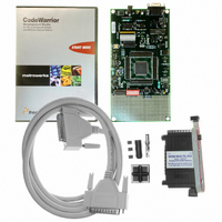
KIT EVALUATION FOR MC912D60A
Manufacturer
Freescale Semiconductor
Type
MCUr
Datasheet
1.M68KIT912D60A.pdf
(11 pages)
Specifications of M68KIT912D60A
Contents
Module and Misc Hardware
Processor To Be Evaluated
68HC912D60A
Data Bus Width
16 bit
Interface Type
RS-232
Silicon Manufacturer
Freescale
Core Architecture
HC12
Core Sub-architecture
HC12
Silicon Core Number
MC68HC912
Rohs Compliant
No
For Use With/related Products
MC912D60A
Lead Free Status / RoHS Status
Contains lead / RoHS non-compliant


M68EVB912D60/D
Freescale Semiconductor, Inc.
3. Hardware Reference
3.1 Power Supply
The EVB requires an external +5 volt power supply for operation. Ideally this should be current limited to 200mA.
Power is supplied to the EVB via the power socket, P6. A 2.5mm power plug has been included in the
M68EVB912D60 kit to allow the user to power the EVB from a standard desktop power supply. To do this the
user should solder insulated wires onto the two terminals of the power plug, and then connect the other ends of
the wires up to their power supply. Great care should be taken to ensure that the 5 Volt supply is connected to
the internal part of the power plug and the Gnd supply is connected to the external barrel of the power plug.
To +5V Supply
To GND Supply
3.2 BDM In Connector
The EVB can be used in conjunction with a suitable Background Debug Mode (BDM) debugger interface, such
as the SDI, and appropriate debugger software. The BDM input to the EVB is via jumper J16. Table 3-1 shows the
pinout for J16.
3.3 MCU Operating Mode
Jumpers J24 and J25 allow the user to select which mode the MCU starts in after reset by controlling the state of
the MODA and MODB pins. The default mode is to pull the MCU MODA and MODB pins to ground. This
results in the MCU starting from reset in either Single Chip or Special Single Chip mode (dependant on the state
of the BKGD pin).
The state of the MODA and MODB pins can also be set via the Noral SDI cable. When this option is used it is
not necessary to install links on jumpers J24 and J25.
3.4 Clock
A 16 MHz oscillator module provides the clock signal to the MCU. Jumper J27 must be installed between pins 1
and 2 (factory default) to configure the clock signal correctly.
3.5 RS-232C Interface
An RS-232C interface is provided on the EVB through a 9 way D type connector, P1. Signal level translation
between the MCU and P1 is provided by an MC145407 RS-232 interface IC (U3) . This is connected to the TxD
and RxD pins of the Serial Communications Interface (SCI) on the MC68HC912D60 via jumpers J11 (TxD) and J9
(RxD). As there are two serial communications interface modules supplied on the MCU, jumpers J9 and J11 can
be used to select between them. The EVB has been configured to act as Data Circuit-terminating Equipment
(DCE). Removing jumpers J8, J10 and J13 allows the user to disable this function if it is not required.
For More Information On This Product,
M68EVB912D60/D
5
Go to: www.freescale.com
Related parts for M68KIT912D60A
Image
Part Number
Description
Manufacturer
Datasheet
Request
R

Part Number:
Description:
Manufacturer:
Freescale Semiconductor, Inc
Datasheet:
Part Number:
Description:
Manufacturer:
Freescale Semiconductor, Inc
Datasheet:
Part Number:
Description:
Manufacturer:
Freescale Semiconductor, Inc
Datasheet:
Part Number:
Description:
Manufacturer:
Freescale Semiconductor, Inc
Datasheet:
Part Number:
Description:
Manufacturer:
Freescale Semiconductor, Inc
Datasheet:
Part Number:
Description:
Manufacturer:
Freescale Semiconductor, Inc
Datasheet:
Part Number:
Description:
Manufacturer:
Freescale Semiconductor, Inc
Datasheet:
Part Number:
Description:
Manufacturer:
Freescale Semiconductor, Inc
Datasheet:
Part Number:
Description:
Manufacturer:
Freescale Semiconductor, Inc
Datasheet:
Part Number:
Description:
Manufacturer:
Freescale Semiconductor, Inc
Datasheet:
Part Number:
Description:
Manufacturer:
Freescale Semiconductor, Inc
Datasheet:
Part Number:
Description:
Manufacturer:
Freescale Semiconductor, Inc
Datasheet:
Part Number:
Description:
Manufacturer:
Freescale Semiconductor, Inc
Datasheet:
Part Number:
Description:
Manufacturer:
Freescale Semiconductor, Inc
Datasheet:
Part Number:
Description:
Manufacturer:
Freescale Semiconductor, Inc
Datasheet: