M68KIT912D60A Freescale Semiconductor, M68KIT912D60A Datasheet - Page 6
M68KIT912D60A
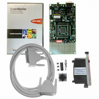
Manufacturer Part Number
M68KIT912D60A
Description
KIT EVALUATION FOR MC912D60A
Manufacturer
Freescale Semiconductor
Type
MCUr
Datasheet
1.M68KIT912D60A.pdf
(11 pages)
Specifications of M68KIT912D60A
Contents
Module and Misc Hardware
Processor To Be Evaluated
68HC912D60A
Data Bus Width
16 bit
Interface Type
RS-232
Silicon Manufacturer
Freescale
Core Architecture
HC12
Core Sub-architecture
HC12
Silicon Core Number
MC68HC912
Rohs Compliant
No
For Use With/related Products
MC912D60A
Lead Free Status / RoHS Status
Contains lead / RoHS non-compliant


3.6 CAN Physical Interface
There is a CAN physical interface supplied on the M68EVB912D60. The CAN physical interface comprises a
Philips PCA82C250 CAN Interface controller (U1). The TXD and RXD pins on the PCA82C250 are connected to
the CANTX and CANRX pins on the MC68HC912D60 respectively. The CAN bus signals, CANH and CANL are
available on jumper J1. Table 3-1 shows the pinout for J1.
3.7 Programming Operation
It is possible to configure the M68EVB912D60 as a programming tool. To do this the relevant programming
adapter board has to be purchased (contact Motorola for further details). To configure the EVB as a programming
tool, the adapter board has to be connected to the header strips on the EVB (when doing this care should be
taken to ensure that the adapter board is installed with the correct polarity as failure to do so could result in
damage to the device being programmed). It is also necessary to install the jumpers on header P8 in the PGMR
position.
There are two possible ways of supplying the flash EEPROM programming voltage V
MAX662 chargepump I.C. (U5), or via the SDI cable. The source of the flash EEPROM programming voltage can
be selected via jumper J17.
There is an option for controlling the operation of the chargepump I.C. (U5). If there is no jumper link installed on
Jumper J14, then the V
will be supplied to the V
the operation of the chargepump I.C. via a port pin of their choice. To do this the user must connect a wire
between the pad situated to the right hand side of Jumper J14 and the pad of the port pin they want to use as the
controller. When this option is chosen the user must remove the jumper link from jumper J14.
3.8 Jumper Configuration
Table 3-1 summarises the jumper and header configurations for the EVB.
Key to Table 3-1
M68EVB912D60/D
2 pin header with no jumper installed
2 pin header with jumper installed
3 pin header with jumper installed between pins 1 and 2
3 pin header with jumper installed between pins 2 and 3
3 pin header with no jumper installed
FP
FP
supply will be held at the level of V
pin of the MCU. In addition to this there is an option which allows the user to control
Freescale Semiconductor, Inc.
J14
For More Information On This Product,
Go to: www.freescale.com
6
From user specified port pin
DD
. If a jumper link is installed on Jumper J14 then 12V
M68EVB912D60/D
FP
to the MCU, either via the
Related parts for M68KIT912D60A
Image
Part Number
Description
Manufacturer
Datasheet
Request
R

Part Number:
Description:
Manufacturer:
Freescale Semiconductor, Inc
Datasheet:
Part Number:
Description:
Manufacturer:
Freescale Semiconductor, Inc
Datasheet:
Part Number:
Description:
Manufacturer:
Freescale Semiconductor, Inc
Datasheet:
Part Number:
Description:
Manufacturer:
Freescale Semiconductor, Inc
Datasheet:
Part Number:
Description:
Manufacturer:
Freescale Semiconductor, Inc
Datasheet:
Part Number:
Description:
Manufacturer:
Freescale Semiconductor, Inc
Datasheet:
Part Number:
Description:
Manufacturer:
Freescale Semiconductor, Inc
Datasheet:
Part Number:
Description:
Manufacturer:
Freescale Semiconductor, Inc
Datasheet:
Part Number:
Description:
Manufacturer:
Freescale Semiconductor, Inc
Datasheet:
Part Number:
Description:
Manufacturer:
Freescale Semiconductor, Inc
Datasheet:
Part Number:
Description:
Manufacturer:
Freescale Semiconductor, Inc
Datasheet:
Part Number:
Description:
Manufacturer:
Freescale Semiconductor, Inc
Datasheet:
Part Number:
Description:
Manufacturer:
Freescale Semiconductor, Inc
Datasheet:
Part Number:
Description:
Manufacturer:
Freescale Semiconductor, Inc
Datasheet:
Part Number:
Description:
Manufacturer:
Freescale Semiconductor, Inc
Datasheet: