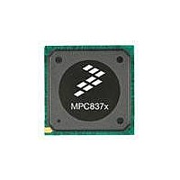
MPC8377E-RDBA Freescale Semiconductor, MPC8377E-RDBA Datasheet - Page 13

MPC8377E-RDBA
Manufacturer Part Number
MPC8377E-RDBA
Description
BOARD REF DES MPC8377 REV 2.1
Manufacturer
Freescale Semiconductor
Series
PowerQUICC II™ PROr
Type
MPUr
Datasheets
1.MPC8377EVRAGD.pdf
(126 pages)
2.MPC8377EVRAGD.pdf
(2 pages)
3.MPC8377E-RDBA.pdf
(2 pages)
Specifications of MPC8377E-RDBA
Design Resources
MPC8379E-RDB Ref Design Guide
Contents
Board, CD
Frequency
667 MHz
For Use With/related Products
MPC8377E
Lead Free Status / RoHS Status
Lead free / RoHS Compliant
- Current page: 13 of 126
- Download datasheet (3Mb)
4
This section provides the clock input DC and AC electrical characteristics for the MPC8377E. Note that
the PCI_CLK/PCI_SYNC_IN signal or CLKIN signal is used as the PCI input clock depending on
whether the device is configured as a host or agent device. CLKIN is used when the device is in host mode.
4.1
Table 7
Freescale Semiconductor
Input high voltage
Input low voltage
CLKIN Input current
PCI_CLK Input current
Note:
1
eTSEC I/O
Load =
25 pf
USB
(60MHz
Clock)
SerDes
Other I/O
Note: The values given are for typical, and not worst case, switching.
Interface
In PCI agent mode, this specification does not comply with PCI 2.3 Specification.
Clock Input Timing
provides the clock input (CLKIN/PCI_CLK) DC timing specifications for the device.
Parameter
DC Electrical Characteristics
MII or RMII
RGMII or
RTBI
12 Mbps
480 Mbps
per lane
Parameter
—
MPC8377E PowerQUICC II Pro Processor Hardware Specifications, Rev. 4
Table 6. MPC8377E Typical I/O Power Dissipation (continued)
(1.8 V)
GV
—
—
—
—
—
—
OV
DD
Table 7. CLKIN DC Electrical Characteristics
DD
0 V ≤ V
0 V ≤ V
– 0.5 V ≤ V
GV
Condition
DD
(2.5 V)
IN
IN
—
—
—
—
—
—
—
—
/LBV
≤ 0.5 V or
≤ OV
IN
DD
DD
≤ OV
(3.3 V)
OV
DD
0.01
0.01
0.2
—
—
DD
(3.3 V)
LV
0.02
Symbol
—
—
—
—
—
DD
V
V
I
I
IN
IN
IH
IL
(2.5 V)
LV
0.05
—
—
—
—
—
DD
–0.3
Min
L[1,2]_nV
2.7
—
—
(1.0 V)
0.029
—
—
—
—
—
DD
OV
DD
Max
± 10
± 30
0.4
Unit
+ 0.3
W
W
W
W
W
W
Multiply by
number of
interfaces used.
Clock Input Timing
Comments
Unit
μA
μA
V
V
—
—
—
—
Notes
—
—
1
1
13
Related parts for MPC8377E-RDBA
Image
Part Number
Description
Manufacturer
Datasheet
Request
R
Part Number:
Description:
BOARD MODULAR DEV SYSTEM
Manufacturer:
Freescale Semiconductor
Datasheet:
Part Number:
Description:
PowerQUICC II Pro Processor
Manufacturer:
Freescale Semiconductor
Part Number:
Description:
Manufacturer:
Freescale Semiconductor, Inc
Datasheet:
Part Number:
Description:
Manufacturer:
Freescale Semiconductor, Inc
Datasheet:
Part Number:
Description:
Manufacturer:
Freescale Semiconductor, Inc
Datasheet:
Part Number:
Description:
Manufacturer:
Freescale Semiconductor, Inc
Datasheet:
Part Number:
Description:
Manufacturer:
Freescale Semiconductor, Inc
Datasheet:
Part Number:
Description:
Manufacturer:
Freescale Semiconductor, Inc
Datasheet:
Part Number:
Description:
Manufacturer:
Freescale Semiconductor, Inc
Datasheet:
Part Number:
Description:
Manufacturer:
Freescale Semiconductor, Inc
Datasheet:
Part Number:
Description:
Manufacturer:
Freescale Semiconductor, Inc
Datasheet:
Part Number:
Description:
Manufacturer:
Freescale Semiconductor, Inc
Datasheet:
Part Number:
Description:
Manufacturer:
Freescale Semiconductor, Inc
Datasheet:
Part Number:
Description:
Manufacturer:
Freescale Semiconductor, Inc
Datasheet:
Part Number:
Description:
Manufacturer:
Freescale Semiconductor, Inc
Datasheet:


