DK-SI-4SGX230N Altera, DK-SI-4SGX230N Datasheet - Page 15
DK-SI-4SGX230N
Manufacturer Part Number
DK-SI-4SGX230N
Description
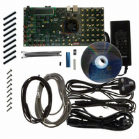
KIT DEV STRATIX IV 4SGX230N/C2
Manufacturer
Altera
Series
Stratix® IV GXr
Type
FPGAr
Datasheet
1.DK-SI-4SGX230N.pdf
(30 pages)
Specifications of DK-SI-4SGX230N
Contents
Board, Cables, CD, Power Supply
Silicon Manufacturer
Altera
Core Architecture
FPGA
Core Sub-architecture
Stratix
Silicon Core Number
EP4S
Silicon Family Name
Stratix IV GX
Rohs Compliant
Yes
For Use With/related Products
EP4SGX230
Lead Free Status / RoHS Status
Lead free / RoHS Compliant
Other names
544-2592
DK-SI-4SGX230N/C2
DK-SI-4SGX230N/C2
Available stocks
Company
Part Number
Manufacturer
Quantity
Price


Introduction
Test Designs
Table 6–1. Data Rates for Test Designs
Configuring the FPGA Using Quartus II Programmer
© February 2009 Altera Corporation
signal_integrity_demo1.sof
signal_integrity_demo2.sof
signal_integrity_demo3.sof
Note to
(1) The clock input is expected from the socketed oscillator (Y3) (soc_clk) on the board. If you are targeting –2 speed grade device on the board,
you can use 425 MHz. For –3 speed grade, the maximum data rate limit supported is 6.5 Gbps. Therefore, you must use 312.5 MHz (312.5*20
< 6.5 Gbps) and not the 425-MHz clock crystal.
Table
File Name
6–1:
The kit installs a demonstration application and test designs. The application
provides an easy-to-use interface where you can select various transceiver settings
and observe the result. Before you run the application and test designs, connect the
USB cable to the board and navigate to the Stratix IV GX Transceiver Signal Integrity
Demonstration application as explained in
Development Kit, Stratix IV GX Edition CD-ROM” on page
Altera provides a set of test designs for the evaluation of the Stratix IV GX device
transceiver performance and board features. The .sof file names and data rates for
each test design are listed in
Quartus II Programmer to configure the Stratix IV GX device with one of the .sof files.
It is sometimes necessary to use the Quartus II Programmer to configure the FPGA
with specific .sof files, such as the designs in
ensure that the Quartus II Programmer and the USB-Blaster driver are installed on the
host computer and the development board is powered up.
To configure the Stratix IV GX FPGA, perform the following steps:
1. Start the Quartus II Programmer.
2. Click Add File and select the path to the desired .sof.
3. Turn on the Program/Configure option for the added file.
soc_clk*20
soc_clk*20
Transceiver
Channel 0
Data Rate
Refer to
Block 0
(Gbps)
transceiver channel data rates and functional modes.
(1)
(1)
“Channel Reconfig Tab” on page 6–7
soc_clk*20
Transceiver
Channel 1,
Channel 2
Data Rate
Block 1
(Gbps)
3.125
Table
Transceiver Signal Integrity Development Kit, Stratix IV GX Edition User Guide
6. Stratix IV GX Transceiver Signal
(1)
6–1. Before you run the application, use the
(Gen1 or Gen2)
soc_clk*20
Transceiver
PCI Express
Channel 3,
Channel 4
Data Rate
Block 1
(Gbps)
“Installing the Transceiver Signal Integrity
Table
Integrity Demonstration
(1)
for the available
6–1. Before configuring the FPGA,
soc_clk*20
soc_clk*20
Transceiver
Channel 7
Data Rate
Block 2
(Gbps)
3–1.
(1)
(1)
external SMA clock
Clocking scheme
socket clock or
(J19 and J20)
socket clock
socket clock
Related parts for DK-SI-4SGX230N
Image
Part Number
Description
Manufacturer
Datasheet
Request
R

Part Number:
Description:
SI KIT W/SII GX EP2SGX90N
Manufacturer:
Altera
Datasheet:

Part Number:
Description:
KIT DEV STRATIX IV TRANSCEIVER
Manufacturer:
Altera
Datasheet:

Part Number:
Description:
KIT DEV STRATIX V FPGA 5SGXEA7
Manufacturer:
Altera
Datasheet:

Part Number:
Description:
Programmable Logic IC Development Tools FPGA Starter Kit For Stratix V 5SGXEA7
Manufacturer:
Altera Corporation
Part Number:
Description:
Programmable Logic IC Development Tools FPGA Starter Kit For Stratix V 5SGTMC7
Manufacturer:
Altera Corporation
Part Number:
Description:
Programmable Logic IC Development Tools FPGA Starter Kit For Stratix V 5SGTMC7 ES
Manufacturer:
Altera Corporation

Part Number:
Description:
CYCLONE II STARTER KIT EP2C20N
Manufacturer:
Altera
Datasheet:
Part Number:
Description:
CPLD, EP610 Family, ECMOS Process, 300 Gates, 16 Macro Cells, 16 Reg., 16 User I/Os, 5V Supply, 35 Speed Grade, 24DIP
Manufacturer:
Altera Corporation
Datasheet:
Part Number:
Description:
CPLD, EP610 Family, ECMOS Process, 300 Gates, 16 Macro Cells, 16 Reg., 16 User I/Os, 5V Supply, 15 Speed Grade, 24DIP
Manufacturer:
Altera Corporation
Datasheet:
Part Number:
Description:
Manufacturer:
Altera Corporation
Datasheet:
Part Number:
Description:
CPLD, EP610 Family, ECMOS Process, 300 Gates, 16 Macro Cells, 16 Reg., 16 User I/Os, 5V Supply, 30 Speed Grade, 24DIP
Manufacturer:
Altera Corporation
Datasheet:
Part Number:
Description:
High-performance, low-power erasable programmable logic devices with 8 macrocells, 10ns
Manufacturer:
Altera Corporation
Datasheet:
Part Number:
Description:
High-performance, low-power erasable programmable logic devices with 8 macrocells, 7ns
Manufacturer:
Altera Corporation
Datasheet: