HW-V5-ML550-UNI-G Xilinx Inc, HW-V5-ML550-UNI-G Datasheet - Page 74
HW-V5-ML550-UNI-G
Manufacturer Part Number
HW-V5-ML550-UNI-G
Description
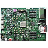
EVALUATION PLATFORM VIRTEX-5
Manufacturer
Xilinx Inc
Series
Virtex™-5 LXTr
Type
FPGAr
Datasheet
1.HW-V5-ML550-UNI-G.pdf
(88 pages)
Specifications of HW-V5-ML550-UNI-G
Contents
Development Platform, Power Supply, Loopback Board, CompactFlash Card, software and documentation
Silicon Manufacturer
Xilinx
Features
64M X 8 DDR SDRAM Memory, Six Samtec LVDS Connectors
Kit Contents
Board, Cable, PSU, CD, Docs
Silicon Family Name
Virtex-5
Silicon Core Number
XC5VLX50T-FFG1136
Rohs Compliant
Yes
Lead Free Status / RoHS Status
Lead free / RoHS Compliant
For Use With/related Products
Virtex™-5 LXT
Lead Free Status / RoHS Status
Lead free / RoHS Compliant, Lead free / RoHS Compliant
Available stocks
Company
Part Number
Manufacturer
Quantity
Price


Appendix C: LCD Interface
74
Because of these default settings, the following display controller connections are not used:
When RESETB is Low, the display controller is initialized as indicated in
Table C-4: Display Controller Initialization (RESETB is Low)
When RESETB is High, the display must be initialized. The first steps to be taken to
guarantee correct operation of the display and the controller are:
Display
Entire display
ADC select
Reverse display
Power control
LCD bias
Read-modify-write
SHL select
Static indicator mode
Static indicator register
Display start
Column address
Page address
Regulator select
Reference voltage
Reference Voltage register
Normal power mode is set
The voltage follower and voltage regulator are set to:
DISP: Turns into an output when Master mode is selected
FRS: Static driver segment output
M: Used in Master/Slave display configurations
CL: Clock pin used in Master/Slave display configurations
Configure the ADC bit. This bit determines the scanning direction of the segments.
Configure the SHL bit. This bit sets the scanning direction of the COM lines.
Five times boost mode
The V4, V3, V2, V1, and V0 outputs depend on the bias settings of 1/9 or 1/7.
When the RESETB signal is active, ADC is reset to 0, meaning that the segments
are scanned from SEG1 up to SEG132.
When ADC is set to 1, the segments are scanned in opposite direction.
When the RESETB signal is active, SHL is reset to 0, meaning that the segments
are scanned from COM1 up to COM64.
Parameter
www.xilinx.com
OFF
OFF
OFF
OFF
0,0,0 (VC, VR, VF)
1/7
OFF
OFF
OFF
0,0 (S1, S0)
0 (First line)
0
0
0,0,0 (R2, R1, R0)
OFF
1,0,0,0,0,0 (SV5, SV4, SV3, SV2, SV1, SV0)
Initial Value
ML550 Networking Interfaces Platform
UG202 (v1.4) April 18, 2008
Table
C-4.
R
Related parts for HW-V5-ML550-UNI-G
Image
Part Number
Description
Manufacturer
Datasheet
Request
R

Part Number:
Description:
IC CPLD .8K 36MCELL 44-VQFP
Manufacturer:
Xilinx Inc
Datasheet:

Part Number:
Description:
IC CPLD 72MCRCELL 10NS 44VQFP
Manufacturer:
Xilinx Inc
Datasheet:

Part Number:
Description:
IC CPLD 1.6K 72MCELL 64-VQFP
Manufacturer:
Xilinx Inc
Datasheet:

Part Number:
Description:
IC CR-II CPLD 64MCELL 44-VQFP
Manufacturer:
Xilinx Inc
Datasheet:

Part Number:
Description:
IC CPLD 1.6K 72MCELL 100-TQFP
Manufacturer:
Xilinx Inc
Datasheet:

Part Number:
Description:
IC CR-II CPLD 64MCELL 56-BGA
Manufacturer:
Xilinx Inc
Datasheet:

Part Number:
Description:
IC CPLD 72MCRCELL 7.5NS 44VQFP
Manufacturer:
Xilinx Inc
Datasheet:
Part Number:
Description:
IC CR-II CPLD 64MCELL 100-VQFP
Manufacturer:
Xilinx Inc
Datasheet:
Part Number:
Description:
IC CPLD 1.6K 72MCELL 100-TQFP
Manufacturer:
Xilinx Inc
Datasheet:

Part Number:
Description:
IC CPLD 72MCRCELL 7.5NS 64VQFP
Manufacturer:
Xilinx Inc
Datasheet:
Part Number:
Description:
IC CPLD 1.6K 72MCELL 100-TQFP
Manufacturer:
Xilinx Inc
Datasheet:

Part Number:
Description:
IC CPLD 1.5K 64MCELL HP 44-VQFP
Manufacturer:
Xilinx Inc

Part Number:
Description:
IC CPLD 36MCRCELL 15NS 44PLCC
Manufacturer:
Xilinx Inc
Datasheet:

Part Number:
Description:
IC CPLD 36MCRCELL 10NS 44PLCC
Manufacturer:
Xilinx Inc
Datasheet:

Part Number:
Description:
IC CPLD 1.5K 64MCELL HP 44-VQFP
Manufacturer:
Xilinx Inc