HW-V5-ML550-UNI-G Xilinx Inc, HW-V5-ML550-UNI-G Datasheet - Page 81
HW-V5-ML550-UNI-G
Manufacturer Part Number
HW-V5-ML550-UNI-G
Description
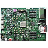
EVALUATION PLATFORM VIRTEX-5
Manufacturer
Xilinx Inc
Series
Virtex™-5 LXTr
Type
FPGAr
Datasheet
1.HW-V5-ML550-UNI-G.pdf
(88 pages)
Specifications of HW-V5-ML550-UNI-G
Contents
Development Platform, Power Supply, Loopback Board, CompactFlash Card, software and documentation
Silicon Manufacturer
Xilinx
Features
64M X 8 DDR SDRAM Memory, Six Samtec LVDS Connectors
Kit Contents
Board, Cable, PSU, CD, Docs
Silicon Family Name
Virtex-5
Silicon Core Number
XC5VLX50T-FFG1136
Rohs Compliant
Yes
Lead Free Status / RoHS Status
Lead free / RoHS Compliant
For Use With/related Products
Virtex™-5 LXT
Lead Free Status / RoHS Status
Lead free / RoHS Compliant, Lead free / RoHS Compliant
Available stocks
Company
Part Number
Manufacturer
Quantity
Price


ML550 Networking Interfaces Platform
UG202 (v1.4) April 18, 2008
R
WData (32+4)
Address
Write
Enable
Clock
RData (8+gnd)
LCD Panel Used in Character Mode
Figure C-8: General Block Diagram of Panel in Full Graphics Mode
This design example requires a byte representing a command or data to be displayed as
input.
Display Command Byte
The command set of the display can be found in
When the LCD interface is enabled for the first time, a set of command bytes is sent to the
LCD. This command set provides the basic initialization of the LCD display controller.
When this initialization is done, the normal LCD display interface is freed for normal use.
Command bytes from the valid command set can be sent to the display (controller).
A detailed description of the LCD controller interface can be found in the
Toplevel.vhd.txt file.
Design for Full Graphics Interface, Attached to CoreConnect Bus
When the Enable signal is Low, nothing happens. The display interface design is
locked.
When the Enable signal is High and the “data_or_command” control signal is Low,
the byte written is a display command.
When the Enable signal and the data_or_command control signal are High, the byte
written is the ASCII character code of the character to be put on the display.
IorD = '1' Instruction
Block RAM
Clock
Reset
'0' Data
E
www.xilinx.com
TC
IorD (bit 9)
Addr
read
ena
Clock
DataOut (8)
DataIn (8)
Table
C-7.
Hardware Schematic Diagram
Clock
Clock
Reset
UG202_C_08_050906
Machine
State
DB (8)
CS1B
RS
RW
E
81
Related parts for HW-V5-ML550-UNI-G
Image
Part Number
Description
Manufacturer
Datasheet
Request
R

Part Number:
Description:
IC CPLD .8K 36MCELL 44-VQFP
Manufacturer:
Xilinx Inc
Datasheet:

Part Number:
Description:
IC CPLD 72MCRCELL 10NS 44VQFP
Manufacturer:
Xilinx Inc
Datasheet:

Part Number:
Description:
IC CPLD 1.6K 72MCELL 64-VQFP
Manufacturer:
Xilinx Inc
Datasheet:

Part Number:
Description:
IC CR-II CPLD 64MCELL 44-VQFP
Manufacturer:
Xilinx Inc
Datasheet:

Part Number:
Description:
IC CPLD 1.6K 72MCELL 100-TQFP
Manufacturer:
Xilinx Inc
Datasheet:

Part Number:
Description:
IC CR-II CPLD 64MCELL 56-BGA
Manufacturer:
Xilinx Inc
Datasheet:

Part Number:
Description:
IC CPLD 72MCRCELL 7.5NS 44VQFP
Manufacturer:
Xilinx Inc
Datasheet:
Part Number:
Description:
IC CR-II CPLD 64MCELL 100-VQFP
Manufacturer:
Xilinx Inc
Datasheet:
Part Number:
Description:
IC CPLD 1.6K 72MCELL 100-TQFP
Manufacturer:
Xilinx Inc
Datasheet:

Part Number:
Description:
IC CPLD 72MCRCELL 7.5NS 64VQFP
Manufacturer:
Xilinx Inc
Datasheet:
Part Number:
Description:
IC CPLD 1.6K 72MCELL 100-TQFP
Manufacturer:
Xilinx Inc
Datasheet:

Part Number:
Description:
IC CPLD 1.5K 64MCELL HP 44-VQFP
Manufacturer:
Xilinx Inc

Part Number:
Description:
IC CPLD 36MCRCELL 15NS 44PLCC
Manufacturer:
Xilinx Inc
Datasheet:

Part Number:
Description:
IC CPLD 36MCRCELL 10NS 44PLCC
Manufacturer:
Xilinx Inc
Datasheet:

Part Number:
Description:
IC CPLD 1.5K 64MCELL HP 44-VQFP
Manufacturer:
Xilinx Inc