8.10.00 J-TRACE ARM Segger Microcontroller Systems, 8.10.00 J-TRACE ARM Datasheet - Page 182
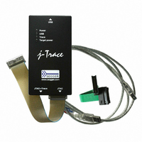
8.10.00 J-TRACE ARM
Manufacturer Part Number
8.10.00 J-TRACE ARM
Description
JTAG EMULATOR ARM7/ARM9 ETM
Manufacturer
Segger Microcontroller Systems
Type
Emulatorr
Specifications of 8.10.00 J-TRACE ARM
Contents
Emulation Module
For Use With/related Products
ARM7, ARM9
Lead Free Status / RoHS Status
Lead free / RoHS Compliant
Other names
899-1006


182
8.3
J-Link / J-Trace (UM08001)
J-Trace provides a JTAG/SWD+Trace connector. This
connector is a 19-pin connector. It connects to the
target via an 1-1 cable.
The following table lists the J-Link / J-Trace SWD pinout.
Table 8.8: 19-pin JTAG/SWD and Trace pinout
8
9
10
11
12
13
14
PIN
1
2
4
6
--- ---
19-pin JTAG/SWD and Trace connector
VTref
SWDIO/
TMS
SWCLK/TCK Output
SWO/TDO
TDI
NC
nRESET
5V-Supply
TRACECLK
5V-Supply
TRACE-
DATA[0]
SIGNAL
Input
I/O /
output
Input
---
Output
NC
I/O
Output
Input
Output
Input
TYPE
This is the target reference voltage. It is used to check if
the target has power, to create the logic-level reference
for the input comparators and to control the output logic
levels to the target. It is normally fed from Vdd of the
target board and must not have a series resistor.
JTAG mode set input of target CPU. This pin should be
pulled up on the target. Typically connected to TMS of the
target CPU.
JTAG clock signal to target CPU. It is recommended that
this pin is pulled to a defined state of the target board.
Typically connected to TCK of the target CPU.
JTAG data output from target CPU. Typically connected to
TDO of the target CPU. When using SWD, this pin is used
as Serial Wire Output trace port. (Optional, not required
for SWD communication)
This pin (normally pin 7) is not existent on the 19-pin
JTAG/SWD and Trace connector.
JTAG data input of target CPU.- It is recommended that
this pin is pulled to a defined state on the target board.
Typically connected to TDI of the target CPU. For CPUs
which do not provide TDI (SWD-only devices), this pin is
not used. J-Link will ignore the signal on this pin when
using SWD.
Not connected inside J-Link. Leave open on target hard-
ware.
Target CPU reset signal. Typically connected to the RESET
pin of the target CPU, which is typically called "nRST",
"nRESET" or "RESET".
This pin can be used to supply power to the target hard-
ware. For more information about how to enable/disable
the power supply, please refer to Target power supply on
page 183.
Input trace clock. Trace clock = 1/2 CPU clock.
This pin can be used to supply power to the target hard-
ware. For more information about how to enable/disable
the power supply, please refer to Target power supply on
page 183.
Input Trace data pin 0.
CHAPTER 8
© 2004-2011 SEGGER Microcontroller GmbH & Co. KG
Description
VTref
GND
GND
- - -
NC
5V-Supply
5V-Supply
GND
GND
GND
Target interfaces and adapters
11
13
15
17
19
1
3
5
7
9
2
12
14
16
18
20
4
6
8
10
SWCLK/TCK
SWO/TDO
TDI
nRESET
TRACECLK
TRACEDATA[0]
TRACEDATA[1]
TRACEDATA[2]
TRACEDATA[3]
SWDIO/TMS
Related parts for 8.10.00 J-TRACE ARM
Image
Part Number
Description
Manufacturer
Datasheet
Request
R

Part Number:
Description:
CONNECTOR JTAG-ARM ISOLATION
Manufacturer:
Segger Microcontroller Systems
Datasheet:

Part Number:
Description:
ADAPTER ARM TARGET 14PIN RIBBON
Manufacturer:
Segger Microcontroller Systems
Datasheet:

Part Number:
Description:
JTAG EMULATOR FOR ARM CORES
Manufacturer:
Segger Microcontroller Systems
Datasheet:

Part Number:
Description:
JTAG EMULATOR FOR ARM CORES
Manufacturer:
Segger Microcontroller Systems
Datasheet:

Part Number:
Description:
PROGRAMMING TOOL FOR MCU
Manufacturer:
Segger Microcontroller Systems
Datasheet:

Part Number:
Description:
PROGRAMMING TOOL FOR ST7 MCU
Manufacturer:
Segger Microcontroller Systems
Datasheet:

Part Number:
Description:
PROGRAMMING TOOL FOR STM8
Manufacturer:
Segger Microcontroller Systems
Datasheet:

Part Number:
Description:
PROGRAMMER JTAG FOR ARM CORES
Manufacturer:
Segger Microcontroller Systems
Datasheet:

Part Number:
Description:
JTAG EMULATOR USB ETHERNET ARM
Manufacturer:
Segger Microcontroller Systems
Datasheet:

Part Number:
Description:
EMULATOR JTAG/SWD CORTEX M3
Manufacturer:
Segger Microcontroller Systems
Datasheet: