EVAL-AD7731EB Analog Devices Inc, EVAL-AD7731EB Datasheet - Page 36
EVAL-AD7731EB
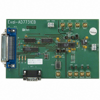
Manufacturer Part Number
EVAL-AD7731EB
Description
BOARD EVAL FOR AD7731
Manufacturer
Analog Devices Inc
Specifications of EVAL-AD7731EB
Number Of Adc's
1
Number Of Bits
24
Sampling Rate (per Second)
6.4k
Data Interface
Serial
Inputs Per Adc
3 Differential
Input Range
±1.28 V
Power (typ) @ Conditions
67.5mW @ 6.4kSPS
Voltage Supply Source
Analog and Digital
Operating Temperature
-40°C ~ 85°C
Utilized Ic / Part
AD7731
Lead Free Status / RoHS Status
Contains lead / RoHS non-compliant


AD7731
CONFIGURING THE AD7731
The AD7731 contains twelve on-chip registers which can be accessed via the serial interface. Figure 5 and Figure 6 have outlined a
flowchart for the reading and writing of these registers. Table XIX and Table XX outline sample pseudo-code for some commonly
used routines. The required operating conditions will dictate the values loaded to the Mode and Filter Registers. The values given
here are for example purposes only.
Write 03 Hex to Serial Port
Write 1332 Hex to Serial Port
Write 02 Hex to Serial Port
Write B174 Hex to Serial Port
Wait for RDY Low
Write 02 Hex to Serial Port
Write 9174 Hex to Serial Port
Wait for RDY Low
1
CHANNEL = 4 Hex
CH_LOOP: MODE = 2177 Hex
MODE = MODE AND CHANNEL
Write 02 Hex to Serial Port
Write MODE to Serial Port
Wait for RDY Low
Write 11 Hex to Serial Port
Read 24-Bit Data From Serial Port
Increment CHANNEL
If CHANNEL = 7Hex Then Set CHANNEL = 4 Hex
Loop to CH_LOOP
This operation is not necessary if the default values of the Filter Register are the values used in the application.
Table XX. Pseudo-Code for Looping AD7731 Through Three Fully-Differential Channels
Table XIX. Pseudo-Code for Initiating a Self-Calibration after Power-On/Reset
1
1
/* Writes to Communications Register Setting Next Operation as Write to
Filter Register*/
/* Writes to Filter Register Setting a 1 kHz Output Rate in nonCHOP
Mode*/
/* Writes to Communications Register Setting Next Operation as Write to
Mode Register*/
/* Writes to Mode Register Initiating Internal Full-Scale Calibration for
0 V to +1.28 V Input Range on Channel Pair AIN1/AIN2*/
/* Wait for RDY pin to go low to indicate end of calibration cycle*/
/* Writes to Communications Register Setting Next Operation as Write to
Mode Register*/
/* Writes to Mode Register Initiating Internal Zero-Scale Calibration for
0 V to +1.28 V Input Range*/
/* Wait for RDY pin to go low to indicate end of calibration cycle*/
/* The part has now completed self-calibration and is in idle mode*/
/* Sets a Variable Called CHANNEL*/
/* Sets a Variable Called MODE */
/* Logical AND of Both Variables */
/* Writes to Communications Register Setting Next Operation as Write to
Mode Register*/
/* Writes to Mode Register Setting Continuous Conversion Mode for 0 V
to +1.28 V Input Range on Channel Determined by CHANNEL Variable*/
/* Wait for RDY pin to go low to Indicate Output Update*/
/* Writes to Communications Register Setting Next Operation as Read
From Data Register*/
/* Read Conversion Result from AD7731’s Data Register*/
/* Increments Channel Address*/
/* Resets Channel Address*/
–36–
REV. A
REV. 0
Related parts for EVAL-AD7731EB
Image
Part Number
Description
Manufacturer
Datasheet
Request
R

Part Number:
Description:
ENERCHIP CC EVAL KIT
Manufacturer:
Cymbet Corporation
Datasheet:

Part Number:
Description:
BOARD EVAL FOR AD976
Manufacturer:
Analog Devices Inc
Datasheet:

Part Number:
Description:
BOARD EVAL FOR ADXL345
Manufacturer:
Analog Devices Inc
Datasheet:

Part Number:
Description:
ENERCHIP CC SEH EVAL KIT
Manufacturer:
Cymbet Corporation
Datasheet:

Part Number:
Description:
ENERCHIP EP ENERGY HARVEST EVAL
Manufacturer:
Cymbet Corporation
Datasheet:

Part Number:
Description:
EVAL BOARD FOR TW6864-LB2-GR
Manufacturer:
Intersil
Datasheet:
Part Number:
Description:
EVAL BOARD FOR TW8816-LB3-GR
Manufacturer:
Intersil
Datasheet:
Part Number:
Description:
EVAL BOARD FOR TW8817-TA3-GRS
Manufacturer:
Intersil
Datasheet:

Part Number:
Description:
EVALUATION MODULE FOR ADUM4160
Manufacturer:
Analog Devices Inc
Datasheet:

Part Number:
Description:
BOARD EVALUATION ADCMP581BCP
Manufacturer:
Analog Devices Inc
Datasheet:
Part Number:
Description:
BOARD EVALUATION ADM1041
Manufacturer:
Analog Devices Inc
Datasheet:

Part Number:
Description:
EVAL BOARD FOR STM32F107VCT
Manufacturer:
STMicroelectronics
Datasheet:
Part Number:
Description:
BOARD EVAL FOR AD1954
Manufacturer:
Analog Devices Inc
Datasheet:
Part Number:
Description:
BOARD EVAL FOR AD1955
Manufacturer:
Analog Devices Inc
Datasheet:

Part Number:
Description:
BOARD EVAL FOR AD7655
Manufacturer:
Analog Devices Inc
Datasheet: