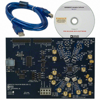
AD9958/PCB Analog Devices Inc, AD9958/PCB Datasheet
AD9958/PCB
Specifications of AD9958/PCB
Available stocks


Related parts for AD9958/PCB


AD9958/PCB Summary of contents
Page 1
FEATURES 2 synchronized DDS channels @ 500 MSPS Independent frequency/phase/amplitude control between channels Matched latencies for frequency/phase/amplitude changes Excellent channel-to-channel isolation (>72 dB) Linear frequency/phase/amplitude sweeping capability levels of frequency/phase/amplitude modulation (pin-selectable) 2 integrated 10-bit digital-to-analog converters ...
Page 2
AD9958 TABLE OF CONTENTS Features .............................................................................................. 1 Applications ....................................................................................... 1 Functional Block Diagram .............................................................. 1 General Description ......................................................................... 3 Specifications ..................................................................................... 4 Absolute Maximum Ratings ............................................................ 8 ESD Caution .................................................................................. 8 Pin Configuration and Function Descriptions ............................. 9 Typical Performance ...
Page 3
GENERAL DESCRIPTION The AD9958 consists of two DDS cores that provide indepen- dent frequency, phase, and amplitude control on each channel. This flexibility can be used to correct imbalances between signals due to analog processing, such as filtering, amplification, or ...
Page 4
AD9958 SPECIFICATIONS AVDD and DVDD = 1.8 V ± 5%; DVDD_I/O = 3.3 V ± 5 25°C; R (REFCLK multiplier bypassed), unless otherwise noted. Table 1. Parameter REFERENCE CLOCK INPUT CHARACTERISTICS Frequency Range REFCLK Multiplier Bypassed REFCLK Multiplier ...
Page 5
Parameter 75.1 MHz Analog Output (±50 kHz) 75.1 MHz Analog Output (±250 kHz) 75.1 MHz Analog Output (±1 MHz) 100.3 MHz Analog Output (±10 kHz) 100.3 MHz Analog Output (±50 kHz) 100.3 MHz Analog Output (±250 kHz) 100.3 MHz Analog ...
Page 6
AD9958 Parameter Residual Phase Noise @ 15.1 MHz (f ) with REFCLK OUT Multiplier Enabled 20× kHz Offset @ 10 kHz Offset @ 100 kHz Offset @ 1 MHz Offset Residual Phase Noise @ 40.1 MHz (f ) ...
Page 7
Parameter POWER SUPPLY Total Power Dissipation—Both Channels On, Single- Tone Mode Total Power Dissipation—Both Channels On, with Sweep Accumulator Total Power Dissipation—Full Power-Down I —Both Channels On, Single-Tone Mode AVDD I —Both Channels On, Sweep Accumulator, AVDD REFCLK Multiplier, and ...
Page 8
AD9958 ABSOLUTE MAXIMUM RATINGS Table 2. Parameter Maximum Junction Temperature DVDD_I/O (Pin 49) AVDD, DVDD Digital Input Voltage (DVDD_I/O = 3.3 V) Digital Output Current Storage Temperature Range Operating Temperature Range Lead Temperature (10 sec Soldering) θ JA θ JC ...
Page 9
PIN CONFIGURATION AND FUNCTION DESCRIPTIONS Table 3. Pin Function Descriptions Pin No. Mnemonic 1 SYNC_IN 2 SYNC_OUT 3 MASTER_RESET 4 PWR_DWN_CTL 5, 7, 11, 15, 19, 21, AVDD 26, 29, 30, 31, 33, 35, 36, 37 10, 12, ...
Page 10
AD9958 Pin No. Mnemonic 24 CLK_MODE_SEL 27 LOOP_FILTER 28, 32, 34 40, 41, 42, 43 P0, P1, P2 I/O_UPDATE SCLK 49 DVDD_I/O 50 SDIO_0 51, 52, 53 SDIO_1, SDIO_2, SDIO_3 54 SYNC_CLK 1 ...
Page 11
TYPICAL PERFORMANCE CHARACTERISTICS DELTA 1 (T1) RBW REF LVL –71.73dB VBW 0dBm 4.50901804MHz SWT 0 –10 –20 –30 –40 –50 –60 –70 –80 –90 –100 START 0Hz 25MHz/DIV Figure 4. Wideband SFDR 1.1 MHz, f OUT DELTA 1 ...
Page 12
AD9958 REF LVL DELTA 1 (T1) RBW 0dBm –84.73dB VBW 254.50901604kHz SWT 0 1 –10 –20 –30 –40 –50 –60 –70 –80 –90 –100 CENTER 1.1MHz 100kHz/DIV Figure 10. NBSFDR 1.1 MHz, f OUT CLK REF LVL DELTA ...
Page 13
FREQUENCY OFFSET (Hz) Figure 16. Residual Phase Noise (SSB) with f OUT 75.1 MHz, 100.3 MHz 500 MHz with REFCLK Multiplier ...
Page 14
AD9958 APPLICATION CIRCUITS AD9958 CH0 CH1 REFCLK Figure 22. Phase Array Radar Using Precision Frequency/Phase Control from DDS in FMCW or Pulsed Radar Applications; REFCLK REFERENCE Figure 24. DDS in PLL Locking to Reference Offering Distribution with Fine Frequency and ...
Page 15
CENTRAL CONTROL Figure 25. Synchronizing Multiple Devices to Increase Channel Capacity Using the AD9510 as a Clock Distributor for the Reference and SYNC_CLK AD9958 REFCLK Figure 26. DDS Providing Stimulus for Acoustic Optical Tunable Filter AD9958 REFCLK Figure 27. Agile ...
Page 16
AD9958 REFCLK Figure 28. Clock Generation Circuit Using the AD9512/AD9513/AD9514/AD9515 Series of Clock Distribution Chips PROGRAMMABLE DIVIDER AND DELAY ADJUST AD9515 CH0 AD9514 AD9513 AD9512 AD9958 AD9515 CH1 IMAGE AD9514 AD9513 AD9512 Rev Page 16 ...
Page 17
EQUIVALENT INPUT AND OUTPUT CIRCUITS DVDD_I/O = 3.3V INPUT OUTPUT AVOID OVERDRIVING DIGITAL INPUTS. FORWARD BIASING DIODES MAY COUPLE DIGITAL NOISE ON POWER PINS. Figure 29. CMOS Digital Inputs CHx_IOUT CHx_IOUT TERMINATE OUTPUTS INTO AVDD. DO NOT EXCEED VOLTAGE COMPLIANCE ...
Page 18
AD9958 THEORY OF OPERATION DDS CORE The AD9958 has two DDS cores, each consisting of a 32-bit phase accumulator and phase-to-amplitude converter. Together, these digital blocks generate a digital sine wave when the phase accumulator is clocked and the phase ...
Page 19
MODES OF OPERATION There are many combinations of modes (for example, single- tone, modulation, linear sweep) that the AD9958 can perform simultaneously. However, some modes require multiple data pins, which can impose limitations. The following guidelines can help determine if ...
Page 20
AD9958 Single-Tone Mode—Matched Pipeline Delay In single-tone mode, the AD9958 offers matched pipeline delay to the DAC input for all frequency, phase, and amplitude changes. This avoids having to deal with different pipeline delays between the three input ports for ...
Page 21
XTAL 39pF Figure 35. Crystal Input Configuration SCALABLE DAC REFERENCE CURRENT CONTROL MODE R is common to all four DACs result, the full-scale SET currents are equal by default. The scalable DAC reference can be used ...
Page 22
AD9958 In modulation mode, the amplitude frequency phase (AFP) select bits (CFR[23:22]) and modulation level bits (FR1[9:8]) are programmed to configure the modulation type and level (see Table 6 and Table 7). Note that the linear sweep enable bit must ...
Page 23
Eight-Level Modulation—No RU/RD The modulation level bits (FR1[9:8]) are set to 10 (eight-level). The AFP select bits (CFR[23:22]) are set to a nonzero value. The RU/RD bits (FR1[11:10]) and the linear sweep enable bit (CFR[14]) are disabled. Note that the ...
Page 24
AD9958 MODULATION USING SDIO_x PINS FOR RU/RD For RU/RD bits = 11, the SDIO_1, SDIO_2, and SDIO_3 pins are available for RU/RD. In this mode, modulation levels and 16 are available. Note that the serial I/O port ...
Page 25
LINEAR SWEEP MODE Linear sweep mode enables the user to sweep frequency, phase, or amplitude from a starting point (S0 endpoint (E0). The purpose of linear sweep mode is to provide better band- width containment compared to direct ...
Page 26
AD9958 This load and countdown operation continues for as long as the timer is enabled. However, the count can be reloaded before reaching 1 by either of the following two methods: • Method change the profile pin. ...
Page 27
OUT FTW1 FTW0 SINGLE-TONE MODE OUT FTW1 FTW0 SINGLE-TONE MODE POINT A: LOAD RISING RAMP RATE REGISTER, APPLY RDW<31:0> AT POINT B: LOAD FALLING RAMP RATE REGISTER, APPLY FDW<31:0> SWEEP AND ...
Page 28
AD9958 OUTPUT AMPLITUDE CONTROL MODE The 10-bit scale factor (multiplier) controls the ramp-up and ramp-down (RU/RD) time of an on/off emission from the DAC. In burst transmissions of digital data, it reduces the adverse spectral impact of abrupt bursts of ...
Page 29
SYNCHRONIZING MULTIPLE AD9958 DEVICES The AD9958 allows easy synchronization of multiple AD9958 devices. At power-up, the phase of SYNC_CLK can be offset between multiple devices. To correct for the offset and align the SYNC_CLK edges, there are three methods (one ...
Page 30
AD9958 I/O_UPDATE, SYNC_CLK, AND SYSTEM CLOCK RELATIONSHIPS I/O_UPDATE and SYNC_CLK are used together to transfer data from the serial I/O buffer to the active registers in the device. Data in the buffer is inactive. SYNC_CLK is a rising edge active ...
Page 31
SERIAL I/O PORT OVERVIEW The AD9958 serial I/O port offers multiple configurations to provide significant flexibility. The serial I/O port offers an SPI- compatible mode of operation that is virtually identical to the SPI operation found in earlier Analog Devices ...
Page 32
AD9958 Each set of communication cycles does not require an I/O update to be issued. The I/O update transfers data from the I/O port buffer to active registers. The I/O update can be sent for each communication cycle or can ...
Page 33
SERIAL I/O MODES OF OPERATION The following are the four programmable modes of serial I/O port operation: • Single-bit serial 2-wire mode (default mode) • Single-bit serial 3-wire mode • 2-bit serial mode • 4-bit serial mode (SYNC_I/O not available) ...
Page 34
AD9958 INSTRUCTION CYCLE CS SCLK SDIO_0 (I0) (I1) (I2) CS SCLK SDIO_1 SDIO_0 (I3) (I4) (I5) (I6) (I7) (D0) Figure 43. Single-Bit Serial Mode Write Timing—Clock Stall Low INSTRUCTION CYCLE DATA ...
Page 35
INSTRUCTION CYCLE CS SCLK SDIO_0 (I0) (I1) (I2) (I3) Figure 46. Single-Bit Serial Mode (2-Wire) Read Timing—Clock Stall High INSTRUCTION CYCLE CS SCLK SDIO_0 (I0) (I1) (I2) (I3) SDO (SDIO_2 PIN) Figure ...
Page 36
AD9958 REGISTER MAPS AND BIT DESCRIPTIONS REGISTER MAPS Table 28. Control Register Map Register Name (Serial Bit Bit 7 Address) Range (MSB) Bit 6 Channel [7:0] Channel 1 Channel 0 1 Select enable enable Register (CSR) (0x00) Function [23:16] VCO ...
Page 37
Table 29. Channel Register Map Register Name (Serial Bit Bit 7 Address) Range (MSB) Bit 6 Channel [23:16] Amplitude freq. phase Function (AFP) select[23:22] 1 Register [15:8] Linear Linear (CFR) sweep sweep (0x03) no-dwell enable [7:0] Digital DAC power- power- ...
Page 38
AD9958 1 Table 30. Profile Register Map Bit Register Name (Address) Range Channel Word 1 (CW1) (0x0A) [31:0] Channel Word 2 (CW2) (0x0B) [31:0] Channel Word 3 (CW3) (0x0C) [31:0] Channel Word 3 (CW4) (0x0D) [31:0] Channel Word 5 (CW5) ...
Page 39
DESCRIPTIONS FOR CONTROL REGISTERS Channel Select Register (CSR)—Address 0x00 One byte is assigned to this register. The CSR determines if channels are enabled or disabled by the status of the two channel enable bits. Both channels are enabled by their ...
Page 40
AD9958 Bit Mnemonic 6 External power-down mode 5 SYNC_CLK disable 4 DAC reference power-down 3:2 Open 1 Manual hardware sync 0 Manual software sync Function Register 2 (FR2)—Address 0x02 Two bytes are assigned to this register. The FR2 is used ...
Page 41
DESCRIPTIONS FOR CHANNEL REGISTERS Channel Function Register (CFR)—Address 0x03 Three bytes are assigned to this register. Table 34. Bit Descriptions for CFR Bit Mnemonic Description 23:22 Amplitude frequency Controls what type of modulation performed for that channel. ...
Page 42
AD9958 Channel Frequency Tuning Word 0 (CFTW0)—Address 0x04 Four bytes are assigned to this register. Table 35. Description for CFTW0 Bit Mnemonic 31:0 Frequency Tuning Word 0 Channel Phase Offset Word 0 (CPOW0)—Address 0x05 Two bytes are assigned to this ...
Page 43
Linear Sweep Ramp Rate (LSRR)—Address 0x07 Two bytes are assigned to this register. Table 38. Description for LSRR Bit Mnemonic 15:8 Falling sweep ramp rate (FSRR) 7:0 Rising sweep ramp rate (RSRR) LSR Rising Delta Word (RDW)—Address 0x08 Four bytes ...
Page 44
... Model Temperature Range 1 AD9958BCPZ −40°C to +85°C 1 AD9958BCPZ-REEL7 −40°C to +85°C 1 AD9958/PCBZ RoHS Compliant Part. ©2005–2008 Analog Devices, Inc. All rights reserved. Trademarks and registered trademarks are the property of their respective owners. 8.00 0.60 MAX 0.60 MAX 43 42 TOP 7 ...