AD9958/PCB Analog Devices Inc, AD9958/PCB Datasheet - Page 36
AD9958/PCB
Manufacturer Part Number
AD9958/PCB
Description
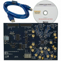
BOARD EVALUATION FOR AD9958
Manufacturer
Analog Devices Inc
Datasheet
1.AD9958BCPZ.pdf
(44 pages)
Specifications of AD9958/PCB
Design Resources
Low Jitter Sampling Clock Generator for High Performance ADCs Using AD9958/9858 and AD9515 (CN0109) Phase Coherent FSK Modulator (CN0186)
Lead Free Status / RoHS Status
Contains lead / RoHS non-compliant
Available stocks
Company
Part Number
Manufacturer
Quantity
Price
Company:

Part Number:
AD9958/PCBZ
Manufacturer:
Analog Devices Inc
Quantity:
135


AD9958
REGISTER MAPS AND BIT DESCRIPTIONS
REGISTER MAPS
Table 28. Control Register Map
Register
Name
(Serial
Address)
Channel
Select
Register
(CSR)
(0x00)
Function
Register 1
(FR1)
(0x01)
Function
Register 2
(FR2)
(0x02)
1
2
In the channel select register, if the user wants two different
frequencies for the two DDS channels, use the following
protocol:
1.
2.
Channel enable bits do not require an I/O update to be activated. These bits are active immediately after the byte containing the bits is written. All other bits need an
I/O update to become active. The two channel enable bits shown in Table 28 are used to enable/disable any combination of the two channels. The default for both
channels is enabled. In readback mode, enable one channel enable bit at a time.
This bit must be disabled (Logic 0) in readback mode.
Enable (Logic 1) the Channel 0 enable bit, which is located
in the channel select register, and disable the Channel 1
enable bit (Logic 0).
Write the desired frequency tuning word for Channel 0, as
described in Step 1, and then disable the Channel 0 enable
bit (Logic 0).
Bit
Range
[7:0]
[23:16]
[15:8]
[7:0]
[15:8]
[7:0]
Bit 7
(MSB)
Channel 1
enable
VCO gain
control
Open
Reference
clock input
power-down
All channels
autoclear
sweep
accumulator
Auto sync
enable
1
Bit 6
Channel 0
enable
External power-
down mode
All channels
clear wweep
accumulator
Multidevice sync
master enable
1
Profile pin configuration (PPC)[14:12]
Bit 5
Open
SYNC_CLK
disable
All channels
autoclear phase
accumulator
Multidevice sync
status
2
Rev. A | Page 36 of 44
PLL divider ratio[22:18]
Bit 4
Open
DAC reference
power-down
All channels
clear phase
accumulator
Multidevice sync
mask
3.
4.
2
Enable the Channel 1 enable bit only, located in the
channel select Register.
Write the desired frequency tuning word for Channel 1 in
Step 3.
Bit 3
Must
be 0
(RU/RD)[11:10]
ramp-down
Ramp-up/
Open[3:2]
Open[3:2]
Bit 2
Serial I/O mode
select[2:1]
Open[11:8]
Bit 1
Manual
hardware
sync
Modulation level[9:8]
Charge pump
control[17:16]
System clock
offset[1:0]
Bit 0
(LSB)
LSB first
Manual
software
sync
Default
Value
0xF0
0x00
0x00
0x00
0x00
0x00
Related parts for AD9958/PCB
Image
Part Number
Description
Manufacturer
Datasheet
Request
R

Part Number:
Description:
BOARD EVALUATION FOR AD9958
Manufacturer:
Analog Devices Inc
Datasheet:


Part Number:
Description:
±1.7g Dual-Axis IMEMS Accelerometer Evaluation Board
Manufacturer:
Analog Devices Inc
Datasheet:

Part Number:
Description:
Inertial Sensor Evaluation System
Manufacturer:
Analog Devices Inc
Datasheet:
Part Number:
Description:
Manufacturer:
Analog Devices Inc
Datasheet:
Part Number:
Description:
Manufacturer:
Analog Devices Inc
Datasheet:
Part Number:
Description:
Manufacturer:
Analog Devices Inc
Datasheet:
Part Number:
Description:
Manufacturer:
Analog Devices Inc
Datasheet:
Part Number:
Description:
Manufacturer:
Analog Devices Inc
Datasheet:
Part Number:
Description:
Manufacturer:
Analog Devices Inc
Datasheet:
Part Number:
Description:
Manufacturer:
Analog Devices Inc
Datasheet:
Part Number:
Description:
Manufacturer:
Analog Devices Inc
Datasheet:
Part Number:
Description:
Manufacturer:
Analog Devices Inc
Datasheet: