AD9958/PCB Analog Devices Inc, AD9958/PCB Datasheet - Page 22
AD9958/PCB
Manufacturer Part Number
AD9958/PCB
Description
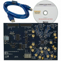
BOARD EVALUATION FOR AD9958
Manufacturer
Analog Devices Inc
Datasheet
1.AD9958BCPZ.pdf
(44 pages)
Specifications of AD9958/PCB
Design Resources
Low Jitter Sampling Clock Generator for High Performance ADCs Using AD9958/9858 and AD9515 (CN0109) Phase Coherent FSK Modulator (CN0186)
Lead Free Status / RoHS Status
Contains lead / RoHS non-compliant
Available stocks
Company
Part Number
Manufacturer
Quantity
Price
Company:

Part Number:
AD9958/PCBZ
Manufacturer:
Analog Devices Inc
Quantity:
135


AD9958
In modulation mode, the amplitude frequency phase (AFP)
select bits (CFR[23:22]) and modulation level bits (FR1[9:8])
are programmed to configure the modulation type and level
(see Table 6 and Table 7). Note that the linear sweep enable bit
must be set to Logic 0 in direct modulation mode.
Table 6. Modulation Type Configuration
AFP Select
(CFR[23:22])
00
01
10
11
Table 7. Modulation Level Selection
Modulation Level (FR1[9:8])
00
01
10
11
When modulating, the RU/RD function can be limited based
on pins available for controlling the feature. The SDIO_x pins
are for RU/RD only, not for modulation.
Table 8. RU/RD Profile Pin Assignments
Ramp-Up/Ramp-Down
(RU/RD) (FR1[11:10])
00
01
10
11
Table 9. Profile Pin Channel Assignments
Profile Pin Configuration (PPC) (FR1[14:12])
XXX
Table 10. Profile Pin and Channel Assignments
Profile Pin Configuration (PPC) (FR1[14:12])
101
Linear Sweep Enable
(CFR[14])
X
0
0
0
Description
RU/RD disabled
Only Profile Pin P2 and Profile Pin P3
available for RU/RD operation
Only Profile Pin P3 available for RU/RD
operation
Only SDIO_1, SDIO_2, and SDIO_3
pins available for RU/RD operation;
this forces the serial I/O to be used
only in 1-bit mode
Description
Modulation disabled
Amplitude modulation
Frequency modulation
Phase modulation
Description
Two-level modulation
Four-level modulation
Eight-level modulation
16-level modulation
P0
CH0
P0
N/A
P1
N/A
P1
CH0
Rev. A | Page 22 of 44
P2
CH0
P2
CH1
If the profile pins are used for RU/RD, Logic 0 is for ramp-up
and Logic 1 is for ramp-down.
Because of the two channels and limited data pins, it is
necessary to assign the profile pins and/or SDIO_1, SDIO_2,
and SDIO_3 pins to a dedicated channel. This is controlled by
the profile pin configuration (PPC) bits (FR1[14:12]). Each of the
following modulation descriptions incorporates data pin
assignments.
Two-Level Modulation—No RU/RD
The modulation level bits (FR1[9:8]) are set to 00 (two-level).
The AFP select bits (CFR[23:22]) are set to the desired modulation
type. The RU/RD bits (FR1[11:10]) and the linear sweep enable
bit (CFR[14]) are disabled. Table 9 displays how the profile pins
and channels are assigned.
As shown in Table 9, only Profile Pin P2 can be used to modulate
Channel 0. If frequency modulation is selected and Profile Pin P2
is Logic 0, Channel Frequency Tuning Word 0 (Register 0x04) is
chosen; if Profile Pin P2 is Logic 1, Channel Word 1 (Register
0x0A) is chosen.
Four-Level Modulation—No RU/RD
The modulation level bits are set to 01 (four-level). The AFP
select bits (CFR[23:22]) are set to the desired modulation type.
The RU/RD bits (FR1[11:10]) and the linear sweep enable bit
(CFR[14]) are disabled. Table 10 displays how the profile pins
and channels are assigned to each other.
For the conditions in Table 10, the profile (channel word)
register chosen is based on the 2-bit value presented to Profile
Pins [P0:P1] or Profile Pins [P2:P3].
For example, if PPC = 101, [P0:P1] = 11, and [P2:P3] = 01, then
the contents of the Channel Word 3 register of Channel 0 are
presented to the output of Channel 0 and the contents of the
Channel Word 1 register of Channel 1 are presented to the
output of Channel 1.
P3
P3
CH1
CH1
Description
Two-level modulation, both channels, no RU/RD
Description
Four-level modulation on CH0 and CH1, no RU/RD
Related parts for AD9958/PCB
Image
Part Number
Description
Manufacturer
Datasheet
Request
R

Part Number:
Description:
BOARD EVALUATION FOR AD9958
Manufacturer:
Analog Devices Inc
Datasheet:


Part Number:
Description:
±1.7g Dual-Axis IMEMS Accelerometer Evaluation Board
Manufacturer:
Analog Devices Inc
Datasheet:

Part Number:
Description:
Inertial Sensor Evaluation System
Manufacturer:
Analog Devices Inc
Datasheet:
Part Number:
Description:
Manufacturer:
Analog Devices Inc
Datasheet:
Part Number:
Description:
Manufacturer:
Analog Devices Inc
Datasheet:
Part Number:
Description:
Manufacturer:
Analog Devices Inc
Datasheet:
Part Number:
Description:
Manufacturer:
Analog Devices Inc
Datasheet:
Part Number:
Description:
Manufacturer:
Analog Devices Inc
Datasheet:
Part Number:
Description:
Manufacturer:
Analog Devices Inc
Datasheet:
Part Number:
Description:
Manufacturer:
Analog Devices Inc
Datasheet:
Part Number:
Description:
Manufacturer:
Analog Devices Inc
Datasheet:
Part Number:
Description:
Manufacturer:
Analog Devices Inc
Datasheet: