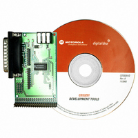
KIT33291DWEVB Freescale Semiconductor, KIT33291DWEVB Datasheet - Page 16

KIT33291DWEVB
Manufacturer Part Number
KIT33291DWEVB
Description
KIT EVAL FOR MC33291 SMART SW
Manufacturer
Freescale Semiconductor
Datasheet
1.MCZ33291EGR2.pdf
(27 pages)
Specifications of KIT33291DWEVB
Main Purpose
Power Management, Low Side Driver (Internal FET)
Embedded
No
Utilized Ic / Part
MC33291
Primary Attributes
8 Channel Internal Switch
Secondary Attributes
Overvoltage, Short-Circuit & Thermal Protection
Lead Free Status / RoHS Status
Contains lead / RoHS non-compliant
SHORT FAULT PROTECT DISABLE (SFPD)
prevent the outputs from latching-off due to an overcurrent
condition. This feature provides control of incandescent lamp
loads where in-rush currents exceed the device’s analog
current limits. Essentially the SFPD pin determines whether
the 33291 output(s) will instantly shut down upon sensing an
output short or remain ON in a current limiting mode of
operation until the output short is removed or thermal
shutdown is reached. If the SFPD pin is tied to V
the 33291 output(s) will remain ON in a current limited mode
of operation upon encountering a load short to supply or
overcurrent condition. When the SFPD pin is grounded, a
short circuit will immediately shut down only the output
affected. Other outputs not having a fault condition will
operate normally. The short circuit operation is addressed in
more detail later.
POWER CONSUMPTION
the operating and standby modes. In the standby, or Sleep,
mode, with V
pin is less than 25 A. In the operating mode, the current
drawn by the VDD pin is less than 4.0 mA (1.0 mA typical)
while the current drawn at the VPWR pin is 2.0 mA maximum
16
33291
FUNCTIONAL DESCRIPTION
FUNCTIONAL PIN DESCRIPTION
The Short Fault Protect Disable (SFPD) pin is used to
The 33291 has extremely low power consumption in both
MCU
DD
Figure 17. Power ON Reset
Reset
2.0 V, the current consumed by the VPWR
V
DD
RDLY
C
DLY
33291
+
Reset
DD
20 A
= 5.0 V
(1.0 mA typical). During normal operation, turning outputs
ON increases I
experiencing a soft short (overcurrent conditions just under
the current limit) adds 0.5 mA to the I
PARALLELING OF OUTPUTS
any combination of outputs together. R
have an inherent positive temperature coefficient providing
balanced current sharing between outputs without
destructive operation (bipolar outputs could not be paralleled
in this fashion as thermal run-away would likely occur). The
device can even be operated with all outputs tied together.
This mode of operation may be desirable in the event the
application requires lower power dissipation or the added
capability of switching higher currents.
corresponding decrease in R
Open Load Detect Currents and the Output Current Limits
increase correspondingly (by a factor of eight if all outputs are
paralleled). Less than 125 m R
limiting of 8 A to 24 A will result if all outputs are paralleled
together. There will be no change in the overvoltage detect or
the OFF output threshold voltage range. The advantage of
paralleling outputs within the same 33291 affords the
existence of minimal R
variation between outputs.
same device is less than 0.5 percent. The variation in clamp
voltages, potentially affecting dynamic current sharing, is less
than five percent. Paralleling outputs from two or more
different devices is possible, but it is not recommended.
There is no guarantee the R
two devices will match. System level thermal design analysis
and verification should be conducted whenever paralleling
outputs, particularly where different devices are involved.
Using MOSFETs as output switches permits connecting
Performance of parallel operation results in a
Typically, the variation of R
PWR
by only 20 A per output. Each output
Analog Integrated Circuit Device Data
DS(ON)
DS(ON)
DS(ON)
and output clamp voltage
DS(ON)
DS(ON)
Freescale Semiconductor
and clamp voltage of the
while the Output OFF
between outputs of the
PWR
DS(ON)
at 25 C with current
current
of MOSFETs


