MT9V022I77ATMH ES Aptina LLC, MT9V022I77ATMH ES Datasheet - Page 5
MT9V022I77ATMH ES
Manufacturer Part Number
MT9V022I77ATMH ES
Description
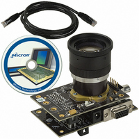
KIT HEAD BOARD FOR MT9V022
Manufacturer
Aptina LLC
Datasheet
1.MT9V022I77ATCH_ES.pdf
(15 pages)
Specifications of MT9V022I77ATMH ES
Lead Free Status / RoHS Status
Lead free / RoHS Compliant
Other names
557-1204


Output Data Timing
Figure 5:
Figure 6:
Table 1:
Serial Bus Description
Register Lock
PDF:09005aef8201ffc3/Source: 09005aef81ff2525
MT9V022_Product_Brief - Rev. A 1/06 EN
Parameter
Nrows
A + Q
P1
P2
A
Q
V
F
Frame Time
Row Timing and FRAME_VALID/LINE_VALID Signals
Timing Example of Pixel Data
Frame start blanking
Note:
Frame end blanking
Horizontal blanking
Vertical blanking
Frame valid time
Total frame time
Active data time
Description
Row time
The data output of the MT9V022 is synchronized with the PIXCLK output. When
LINE_VALID is HIGH, one 10-bit pixel datum is output every PIXCLK period.
Number of master clocks
LINE_VALID
The MT9V022 control registers are written to and read from the two-wire serial interface
bus. The MT9V022 is a serial interface slave with four possible IDs (0x90, 0x98, 0xB0, and
0xB8) determined by S_CTRL_ADR0 and S_CTRL_ADR1 inputs.
Data is transferred into the MT9V022 and out through the serial data (S
S
device can pull the S
device is allowed to pull the S
A register lock feature is included in the MT9V022 to help reduce the probability of an
inadvertent, noise-triggered two-wire serial interface WRITE to the sensor. The user may
lock all registers or only the read mode register. The read mode register controls the
image orientation, and an unintended flip to the image can cause serious results.
FRAME_VALID
DATA
D
OUT
LINE_VALID
PIXCLK
The parameters P1, A, Q, and P2 are defined in Table 1 on page 5.
(9:0)
line is pulled up to V
Blanking
DATA
Pixel Clock
P1
MT9V022: 1/3-Inch Wide-VGA Digital Image Sensor
406,080
444,154
(9:0)
38,074
P 0
752
846
71
23
94
line down. The serial interface protocol determines which
A
DD
DATA
off-chip by a 1. 5kΩ resistor. Either the slave or master
5
(9:0)
P 1
Q
line down at any given time.
Master Clocks
. . .
. . .
. . .
. . .
. . .
. . .
(9:0)
Valid Image Data
Micron Technology, Inc., reserves the right to change products or specifications without notice.
P2
406,080
444,154
38,074
752
846
71
23
94
A
(9:0)
P 3
Q
(9:0)
P 4
A
Time
28.02
31.72
15.23
16.66
2.66
0.86
3.52
1.43
. . . .
. . . .
. . . .
. . . .
. . . .
. . . .
. . . .
. . . .
P2
Output Data Timing
©2006 Micron Technology, Inc. All rights reserved.
P n-1
(9:0)
DATA
(9:0)
P n
) line. The
Units
ms
ms
ms
µs
µs
µs
µs
µs
Blanking
Related parts for MT9V022I77ATMH ES
Image
Part Number
Description
Manufacturer
Datasheet
Request
R

Part Number:
Description:
1/3-Inch Wide-VGA CMOS Digital Image Sensor
Manufacturer:
Aptina Imaging Corporation

Part Number:
Description:
SENSOR IMAGE VGA COLOR CMOS PLCC
Manufacturer:
Aptina LLC
Datasheet:

Part Number:
Description:
IC SENSOR IMAGE COLOR 48CLCC
Manufacturer:
Aptina LLC
Datasheet:

Part Number:
Description:
SENSOR IMAGE 1.3MP CMOS 48-CLCC
Manufacturer:
Aptina LLC
Datasheet:

Part Number:
Description:
SENSOR IMAGE 2MP CMOS 48-CLCC
Manufacturer:
Aptina LLC
Datasheet:

Part Number:
Description:
SENSOR IMAGE VGA MONO 52IBGA
Manufacturer:
Aptina LLC
Datasheet:

Part Number:
Description:
SENSOR IMAGE VGA COLOR 48CLCC
Manufacturer:
Aptina LLC
Datasheet:

Part Number:
Description:
SENSOR IMAGE COLOR CMOS 48-PLCC
Manufacturer:
Aptina LLC
Datasheet:

Part Number:
Description:
KIT HEAD BOARD FOR MT9P031
Manufacturer:
Aptina LLC
Datasheet:

Part Number:
Description:
KIT HEAD BOARD FOR MT9D131
Manufacturer:
Aptina LLC
Datasheet:
Part Number:
Description:
SENSOR IMAGE VGA COLOR CMOS PLCC
Manufacturer:
Aptina LLC
Datasheet:
Part Number:
Description:
IC SENSOR IMAGE COLOR 48CLCC
Manufacturer:
Aptina LLC
Datasheet:
Part Number:
Description:
SENSOR IMAGE 2MP CMOS 48-CLCC
Manufacturer:
Aptina LLC
Datasheet:
