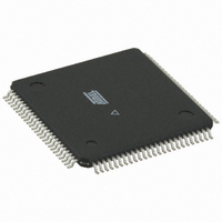
ATMEGA3250P-20AU Atmel, ATMEGA3250P-20AU Datasheet - Page 101

ATMEGA3250P-20AU
Manufacturer Part Number
ATMEGA3250P-20AU
Description
IC MCU AVR 32K FLASH 100-TQFP
Manufacturer
Atmel
Series
AVR® ATmegar
Specifications of ATMEGA3250P-20AU
Core Processor
AVR
Core Size
8-Bit
Speed
20MHz
Connectivity
SPI, UART/USART, USI
Peripherals
Brown-out Detect/Reset, POR, PWM, WDT
Number Of I /o
69
Program Memory Size
32KB (16K x 16)
Program Memory Type
FLASH
Eeprom Size
1K x 8
Ram Size
2K x 8
Voltage - Supply (vcc/vdd)
2.7 V ~ 5.5 V
Data Converters
A/D 8x10b
Oscillator Type
Internal
Operating Temperature
-40°C ~ 85°C
Package / Case
100-TQFP, 100-VQFP
Processor Series
ATMEGA32x
Core
AVR8
Data Bus Width
8 bit
Data Ram Size
2 KB
Interface Type
SPI/UART/USI
Maximum Clock Frequency
20 MHz
Number Of Programmable I/os
69
Number Of Timers
3
Maximum Operating Temperature
+ 85 C
Mounting Style
SMD/SMT
3rd Party Development Tools
EWAVR, EWAVR-BL
Development Tools By Supplier
ATAVRDRAGON, ATSTK500, ATSTK600, ATAVRISP2, ATAVRONEKIT
Minimum Operating Temperature
- 40 C
On-chip Adc
8-ch x 10-bit
For Use With
ATSTK600-TQFP100 - STK600 SOCKET/ADAPTER 100-TQFP770-1007 - ISP 4PORT ATMEL AVR MCU SPI/JTAG770-1005 - ISP 4PORT FOR ATMEL AVR MCU JTAG770-1004 - ISP 4PORT FOR ATMEL AVR MCU SPIATAVRISP2 - PROGRAMMER AVR IN SYSTEMATSTK504 - STARTER KIT AVR EXP MOD 100P LCD
Lead Free Status / RoHS Status
Lead free / RoHS Compliant
Other names
ATMEGA3250P-16AU
ATMEGA3250P-16AU
ATMEGA3250P-16AU
Available stocks
Company
Part Number
Manufacturer
Quantity
Price
Part Number:
ATMEGA3250P-20AU
Manufacturer:
AT
Quantity:
20 000
- Current page: 101 of 364
- Download datasheet (6Mb)
8023F–AVR–07/09
The edge detector generates one clk
(CSn2:0 = 6) edge it detects.
Figure 14-8. T1/T0 Pin Sampling
The synchronization and edge detector logic introduces a delay of 2.5 to 3.5 system clock cycles
from an edge has been applied to the T1/T0 pin to the counter is updated.
Enabling and disabling of the clock input must be done when T1/T0 has been stable for at least
one system clock cycle, otherwise it is a risk that a false Timer/Counter clock pulse is generated.
Each half period of the external clock applied must be longer than one system clock cycle to
ensure correct sampling. The external clock must be guaranteed to have less than half the sys-
tem clock frequency (f
sampling, the maximum frequency of an external clock it can detect is half the sampling fre-
quency (Nyquist sampling theorem). However, due to variation of the system clock frequency
and duty cycle caused by Oscillator source (crystal, resonator, and capacitors) tolerances, it is
recommended that maximum frequency of an external clock source is less than f
An external clock source can not be prescaled.
Figure 14-9. Prescaler for Timer/Counter0 and Timer/Counter1
Note:
PSR10
clk
T0
T1
Tn
I/O
1. The synchronization logic on the input pins (
clk
I/O
Synchronization
Synchronization
D
LE
ExtClk
Q
Synchronization
< f
D
clk_I/O
Q
/2) given a 50/50% duty cycle. Since the edge detector uses
T1
clk
/clk
Clear
T1
T
0
pulse for each positive (CSn2:0 = 7) or negative
T1/T0)
ATmega325P/3250P
is shown in
D
Q
(1)
Figure
Edge Detector
14-8.
clk
T0
clk_I/O
Tn_sync
(To Clock
Select Logic)
/2.5.
101
Related parts for ATMEGA3250P-20AU
Image
Part Number
Description
Manufacturer
Datasheet
Request
R

Part Number:
Description:
Manufacturer:
Atmel Corporation
Datasheet:

Part Number:
Description:
IC AVR MCU 32K 16MHZ 100TQFP
Manufacturer:
Atmel
Datasheet:

Part Number:
Description:
IC AVR MCU 32K 16MHZ 100TQFP
Manufacturer:
Atmel
Datasheet:

Part Number:
Description:
MCU AVR 32K FLASH 16MHZ 100TQFP
Manufacturer:
Atmel
Datasheet:

Part Number:
Description:
Atmega3250 8-bit Microcontroller With In-system Programmable Flash
Manufacturer:
ATMEL Corporation

Part Number:
Description:
Manufacturer:
Atmel Corporation
Datasheet:

Part Number:
Description:
IC AVR MCU 32K 16MHZ 64-QFN
Manufacturer:
Atmel
Datasheet:

Part Number:
Description:
IC AVR MCU 32K 16MHZ 64TQFP
Manufacturer:
Atmel
Datasheet:

Part Number:
Description:
IC AVR MCU 32K 16MHZ 64TQFP
Manufacturer:
Atmel
Datasheet:

Part Number:
Description:
IC AVR MCU 32K 16MHZ 64-QFN
Manufacturer:
Atmel
Datasheet:

Part Number:
Description:
8-bit Microcontroller with In-System Programmable Flash
Manufacturer:
ATMEL [ATMEL Corporation]
Datasheet:

Part Number:
Description:
MCU AVR 32K FLASH 16MHZ 64TQFP
Manufacturer:
Atmel
Datasheet:

Part Number:
Description:
MCU AVR 32K FLASH 16MHZ 64QFN
Manufacturer:
Atmel
Datasheet:


