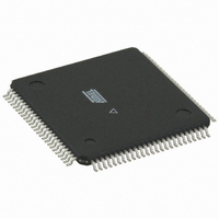
ATMEGA3250P-20AU Atmel, ATMEGA3250P-20AU Datasheet - Page 196

ATMEGA3250P-20AU
Manufacturer Part Number
ATMEGA3250P-20AU
Description
IC MCU AVR 32K FLASH 100-TQFP
Manufacturer
Atmel
Series
AVR® ATmegar
Specifications of ATMEGA3250P-20AU
Core Processor
AVR
Core Size
8-Bit
Speed
20MHz
Connectivity
SPI, UART/USART, USI
Peripherals
Brown-out Detect/Reset, POR, PWM, WDT
Number Of I /o
69
Program Memory Size
32KB (16K x 16)
Program Memory Type
FLASH
Eeprom Size
1K x 8
Ram Size
2K x 8
Voltage - Supply (vcc/vdd)
2.7 V ~ 5.5 V
Data Converters
A/D 8x10b
Oscillator Type
Internal
Operating Temperature
-40°C ~ 85°C
Package / Case
100-TQFP, 100-VQFP
Processor Series
ATMEGA32x
Core
AVR8
Data Bus Width
8 bit
Data Ram Size
2 KB
Interface Type
SPI/UART/USI
Maximum Clock Frequency
20 MHz
Number Of Programmable I/os
69
Number Of Timers
3
Maximum Operating Temperature
+ 85 C
Mounting Style
SMD/SMT
3rd Party Development Tools
EWAVR, EWAVR-BL
Development Tools By Supplier
ATAVRDRAGON, ATSTK500, ATSTK600, ATAVRISP2, ATAVRONEKIT
Minimum Operating Temperature
- 40 C
On-chip Adc
8-ch x 10-bit
For Use With
ATSTK600-TQFP100 - STK600 SOCKET/ADAPTER 100-TQFP770-1007 - ISP 4PORT ATMEL AVR MCU SPI/JTAG770-1005 - ISP 4PORT FOR ATMEL AVR MCU JTAG770-1004 - ISP 4PORT FOR ATMEL AVR MCU SPIATAVRISP2 - PROGRAMMER AVR IN SYSTEMATSTK504 - STARTER KIT AVR EXP MOD 100P LCD
Lead Free Status / RoHS Status
Lead free / RoHS Compliant
Other names
ATMEGA3250P-16AU
ATMEGA3250P-16AU
ATMEGA3250P-16AU
Available stocks
Company
Part Number
Manufacturer
Quantity
Price
Part Number:
ATMEGA3250P-20AU
Manufacturer:
AT
Quantity:
20 000
- Current page: 196 of 364
- Download datasheet (6Mb)
19.3.4
196
ATmega325P/3250P
Two-wire Mode
The USI Two-wire mode is compliant to the Inter IC (TWI) bus protocol, but without slew rate lim-
iting on outputs and input noise filtering. Pin names used by this mode are SCL and SDA.
Figure 19-4. Two-wire Mode Operation, Simplified Diagram
Figure 19-4
It is only the physical layer that is shown since the system operation is highly dependent of the
communication scheme used. The main differences between the Master and Slave operation at
this level, is the serial clock generation which is always done by the Master, and only the Slave
uses the clock control unit. Clock generation must be implemented in software, but the shift
operation is done automatically by both devices. Note that only clocking on negative edge for
shifting data is of practical use in this mode. The slave can insert wait states at start or end of
transfer by forcing the SCL clock low. This means that the Master must always check if the SCL
line was actually released after it has generated a positive edge.
Since the clock also increments the counter, a counter overflow can be used to indicate that the
transfer is completed. The clock is generated by the master by toggling the USCK pin via the
PORT Register.
The data direction is not given by the physical layer. A protocol, like the one used by the TWI-
bus, must be implemented to control the data flow.
SLAVE
MASTER
shows two USI units operating in Two-wire mode, one as Master and one as Slave.
Bit7
Bit7
Bit6
Bit6
Bit5
Bit5
Bit4
Bit4
Bit3
Bit3
Bit2
Bit2
Bit1
Bit1
Bit0
Bit0
Two-wire Clock
Control Unit
PORTxn
HOLD
SCL
SDA
SCL
SDA
SCL
VCC
8023F–AVR–07/09
Related parts for ATMEGA3250P-20AU
Image
Part Number
Description
Manufacturer
Datasheet
Request
R

Part Number:
Description:
Manufacturer:
Atmel Corporation
Datasheet:

Part Number:
Description:
IC AVR MCU 32K 16MHZ 100TQFP
Manufacturer:
Atmel
Datasheet:

Part Number:
Description:
IC AVR MCU 32K 16MHZ 100TQFP
Manufacturer:
Atmel
Datasheet:

Part Number:
Description:
MCU AVR 32K FLASH 16MHZ 100TQFP
Manufacturer:
Atmel
Datasheet:

Part Number:
Description:
Atmega3250 8-bit Microcontroller With In-system Programmable Flash
Manufacturer:
ATMEL Corporation

Part Number:
Description:
Manufacturer:
Atmel Corporation
Datasheet:

Part Number:
Description:
IC AVR MCU 32K 16MHZ 64-QFN
Manufacturer:
Atmel
Datasheet:

Part Number:
Description:
IC AVR MCU 32K 16MHZ 64TQFP
Manufacturer:
Atmel
Datasheet:

Part Number:
Description:
IC AVR MCU 32K 16MHZ 64TQFP
Manufacturer:
Atmel
Datasheet:

Part Number:
Description:
IC AVR MCU 32K 16MHZ 64-QFN
Manufacturer:
Atmel
Datasheet:

Part Number:
Description:
8-bit Microcontroller with In-System Programmable Flash
Manufacturer:
ATMEL [ATMEL Corporation]
Datasheet:

Part Number:
Description:
MCU AVR 32K FLASH 16MHZ 64TQFP
Manufacturer:
Atmel
Datasheet:

Part Number:
Description:
MCU AVR 32K FLASH 16MHZ 64QFN
Manufacturer:
Atmel
Datasheet:


